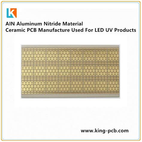
What is an Aluminum Nitride PCB?
An aluminum nitride (AlN) PCB is a specialized type of printed circuit board that uses AlN ceramic as the substrate material instead of the more common FR-4 composite. Aluminum nitride has several unique properties that make it an ideal choice for certain demanding electronics applications:
- High thermal conductivity (up to 285 W/mK, 8-10x higher than alumina)
- Low coefficient of thermal expansion (CTE) close to that of silicon
- Excellent electrical insulation and dielectric strength
- Non-toxic and environmentally friendly
The combination of high heat dissipation, CTE matching, and electrical insulation allows AlN PCBs to operate reliably in high power density and high temperature environments where standard PCBs would fail. Some typical AlN PCB specifications include:
| Property | Value |
|---|---|
| Thermal Conductivity | 170 – 285 W/mK |
| Coefficient of Thermal Expansion | 4.5 ppm/°C |
| Dielectric Constant @ 1 MHz | 8.6 |
| Dielectric Strength | >15 kV/mm |
| Flexural Strength | >300 MPa |
| Density | 3.30 g/cm³ |
Advantages of Aluminum Nitride PCBs
Superior Heat Dissipation
The primary advantage of AlN PCBs is their excellent thermal conductivity, which is 8-10 times higher than alumina (Al2O3) and 100-300 times higher than FR-4. This allows AlN PCBs to efficiently spread and remove heat from power components, reducing operating temperatures and improving reliability. The high thermal conductivity of AlN is due to its unique crystal structure and bonding, which facilitates phonon transport.
Thermal Expansion Matching
AlN has a coefficient of thermal expansion (CTE) of 4.5 ppm/°C, which closely matches that of silicon (2.6 ppm/°C). This minimizes thermomechanical stresses and prevents cracking or delamination when AlN PCBs are subjected to thermal cycling. In contrast, FR-4 has a CTE of 13-16 ppm/°C, which can lead to solder joint failure and component damage under high temperature fluctuations.
Electrical Insulation and High Voltage Capability
Despite its high thermal conductivity, AlN is an excellent electrical insulator with a dielectric strength exceeding 15 kV/mm. This allows AlN PCBs to be used in high voltage applications such as power electronics, where electrical isolation and heat dissipation are both critical. AlN also has a low dielectric constant of 8.6, which minimizes parasitic capacitance and signal loss at high frequencies.
Mechanical Strength and Stability
Aluminum nitride ceramics have high flexural strength (>300 MPa) and fracture toughness, making AlN PCBs resistant to mechanical stress and vibration. AlN also maintains its strength and stiffness at elevated temperatures, unlike polymers such as FR-4 which soften and deform. This dimensional stability is important for precision applications like sensor packaging and laser diode mounting.

Applications of Aluminum Nitride PCBs
Power Electronics
AlN PCBs are widely used in power electronic modules and converters, including insulated gate bipolar transistors (IGBTs), metal-oxide-semiconductor field-effect transistors (MOSFETs), and silicon carbide (SiC) devices. The high thermal conductivity of AlN allows for efficient cooling of these high power density components, while the close CTE match reduces thermomechanical stress during temperature cycling.
Some specific power electronic applications of AlN PCBs include:
- Electric vehicle and hybrid electric vehicle (EV/HEV) inverters
- Motor drives and controls
- Uninterruptible power supplies (UPS)
- Renewable energy converters (solar, wind)
- High voltage DC transmission (HVDC)
RF and Microwave Devices
AlN PCBs are used as substrates for radio frequency (RF) and microwave components operating at frequencies from 1 GHz to over 100 GHz. The low dielectric loss tangent and low CTE of AlN enable stable performance and precise impedance control across wide temperature ranges. AlN also provides effective heat spreading for high power RF devices like gallium nitride (GaN) amplifiers.
Examples of RF/microwave applications using AlN PCBs:
- 5G wireless base stations and antennas
- Radar systems (automotive, aerospace, defense)
- Satellite communications
- Microwave backhaul links
- Test and measurement equipment
LED Lighting and Laser Diodes
High power light-emitting diodes (LEDs) and laser diodes generate significant amounts of heat that must be dissipated to prevent overheating and efficiency loss. AlN PCBs are used as submounts and packages for these optoelectronic devices, providing a low thermal resistance path to heat sinks or cooling systems. The CTE match between AlN and common semiconductor materials (GaN, InGaAsP) reduces strain and improves reliability.
LED and laser applications employing AlN PCBs include:
- Solid-state lighting (SSL) fixtures and lamps
- Automotive headlights and taillights
- Fiber-optic communications (pump lasers, transmitters)
- Industrial lasers for cutting, welding, marking
- Medical lasers (surgery, dermatology, ophthalmology)
Sensors and MEMS Packaging
Aluminum nitride PCBs are used to package microelectromechanical systems (MEMS) sensors that are exposed to harsh environments with high temperatures or corrosive chemicals. The thermal and mechanical stability of AlN protects sensitive MEMS structures from damage or drift, while allowing for hermetic sealing and electrical feedthroughs. AlN also provides a compatible surface for direct bonding or integration of MEMS components.
MEMS sensors packaged with AlN PCBs are found in:
- Automotive exhaust gas sensors (NOx, O2, PM)
- Industrial process monitoring (pressure, flow, pH)
- Oil and gas exploration (downhole logging tools)
- Aerospace engines and fuel systems
- Medical implants and catheters

Fabrication of Aluminum Nitride PCBs
The manufacturing process for AlN PCBs involves several specialized techniques compared to conventional PCBs:
-
AlN Substrate Preparation: Raw AlN powder is mixed with binders, pressed into sheets, and sintered at high temperatures (1700-1900°C) to form dense ceramIC Substrates. The substrates are then ground and polished to achieve the desired thickness and surface finish.
-
Metallization: Conductive traces and pads are formed on the AlN surface by thin-film deposition methods such as sputtering, evaporation, or plating. Common metallization materials include copper, gold, and refractory metals like tungsten or molybdenum for high temperature applications.
-
Patterning: The metal layers are patterned using photolithography and etching processes to define the circuit layout. Fine feature sizes down to 10-50 µm can be achieved with proper process control.
-
Multilayer Lamination: For multilayer AlN PCBs, additional ceramic and metal layers are stacked and laminated together under high pressure and temperature. Conductive vias are formed through the AlN layers to interconnect the different metal levels.
-
Surface Finishing: Optional finishes like nickel/gold (ENIG), silver, or solder may be applied to the AlN PCB surface for improved solderability, wire bonding, or environmental protection.
The key challenges in AlN PCB fabrication include managing the high sintering temperatures, optimizing the metal adhesion and patterning processes, and controlling the residual stresses and warpage of the final PCB Assembly.

Design Considerations for Aluminum Nitride PCBs
When designing circuits on AlN PCBs, several factors must be taken into account:
-
Thermal Management: While AlN has high thermal conductivity, proper heat spreading and cooling paths must still be designed to remove heat from power devices. Thermal vias, metal cores, and external heat sinks can be used to enhance heat transfer.
-
CTE Mismatch: Although AlN closely matches the CTE of silicon, there can still be significant mismatch with other materials like metals or plastics. Designers must analyze and optimize the thermomechanical stresses in AlN PCB assemblies to avoid failures.
-
High Voltage Spacing: For high voltage applications, adequate creepage and clearance distances must be maintained between conductors to prevent arcing or breakdown. AlN PCBs can support higher voltages than FR-4 due to their superior dielectric strength.
-
RF Performance: At high frequencies, the layout and stack-up of AlN PCBs must be carefully designed to control impedance, minimize losses, and suppress electromagnetic interference (EMI). Grounding, shielding, and matching networks are critical for RF circuits.
-
Manufacturability: AlN PCBs have tighter tolerances and design rules compared to FR-4, due to the challenges of ceramic processing and metallization. Designers must work closely with AlN PCB fabricators to ensure their layouts are manufacturable and reliable.
Frequently Asked Questions (FAQ)
What is the typical cost of an AlN PCB compared to FR-4?
AlN PCBs are significantly more expensive than FR-4, due to the higher cost of raw materials and specialized manufacturing processes. The price of an AlN PCB can be 5-20 times higher than an equivalent FR-4 board, depending on the size, complexity, and volume. However, the total system cost may be lower with AlN due to improved performance, reliability, and cooling requirements.
Can AlN PCBs be soldered using standard reflow or Wave Soldering processes?
Yes, AlN PCBs are compatible with standard lead-free soldering processes, as long as the metallization and surface finish are properly designed. The high thermal conductivity of AlN actually helps to reduce thermal gradients and improve solder joint quality. However, the reflow temperature profile may need to be adjusted to account for the different heat transfer characteristics of AlN compared to FR-4.
How do AlN PCBs compare to other Ceramic PCB materials like alumina or beryllia?
Alumina (Al2O3) is the most common ceramic PCB material, but it has lower thermal conductivity (24-30 W/mK) and higher CTE (6-8 ppm/°C) than AlN. Beryllia (BeO) has very high thermal conductivity (270 W/mK) but is toxic and restricted in many applications. AlN offers a balance of high performance, safety, and manufacturability that makes it the preferred choice for most high power and high frequency applications.
What are the environmental and safety considerations for AlN PCBs?
AlN is a non-toxic and environmentally friendly material, unlike beryllia which is harmful to human health. However, the manufacturing process for AlN PCBs involves high temperatures and chemical etching steps that can generate hazardous waste if not properly controlled. AlN PCB fabricators must follow strict environmental and safety regulations to minimize their impact and protect their workers.
What is the future outlook for AlN PCB technology?
The demand for AlN PCBs is expected to grow significantly in the coming years, driven by the increasing power density, frequency, and reliability requirements of emerging applications like electric vehicles, 5G communications, and renewable energy systems. Advances in AlN materials, processing, and design tools will continue to push the boundaries of performance and cost-effectiveness. As more designers become familiar with the benefits of AlN PCBs, they will likely find new and innovative uses for this versatile technology.
No responses yet