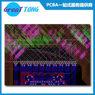
Overview of PCB Design Challenges
PCB design is a complex process that involves multiple stages, from concept to manufacturing. Each stage presents its own set of challenges that must be addressed to ensure the final product meets the required specifications and performs reliably. Some of the key challenges in PCB design include:
- Signal Integrity
- Power Integrity
- Electromagnetic Compatibility (EMC)
- Thermal Management
- Manufacturing Constraints
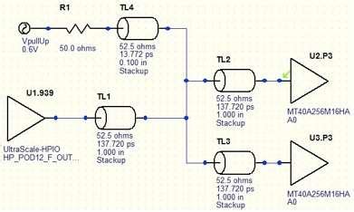
Signal Integrity
Signal integrity is one of the most critical aspects of PCB design. It refers to the ability of a signal to propagate through the PCB without distortion or loss of information. Signal integrity issues can arise due to various factors, such as:
- Impedance mismatches
- Crosstalk
- Reflections
- Attenuation
To address signal integrity challenges, PCB designers must carefully consider factors such as trace geometry, materials, and routing techniques. PCEA provides resources and training to help designers optimize signal integrity in their designs.
Power Integrity
Power integrity is another critical aspect of PCB design. It refers to the ability of the PCB to provide stable and clean power to all components on the board. Power integrity issues can arise due to factors such as:
- Voltage drops
- Ground bounces
- Noise
- Electromagnetic interference (EMI)
To address power integrity challenges, PCB designers must carefully consider factors such as power distribution networks, decoupling capacitors, and grounding techniques. PCEA provides resources and training to help designers optimize power integrity in their designs.
Electromagnetic Compatibility (EMC)
EMC refers to the ability of a PCB to function properly in the presence of electromagnetic interference (EMI) and to not generate EMI that could interfere with other devices. EMC challenges can arise due to factors such as:
- Radiated emissions
- Conducted emissions
- Susceptibility to external EMI
To address EMC challenges, PCB designers must carefully consider factors such as shielding, filtering, and grounding techniques. PCEA provides resources and training to help designers ensure their designs meet EMC requirements.
Thermal Management
Thermal management is an important consideration in PCB design, particularly for high-power applications. Thermal management challenges can arise due to factors such as:
- Power dissipation
- Heat generation
- Cooling limitations
To address thermal management challenges, PCB designers must carefully consider factors such as component placement, thermal vias, and cooling techniques. PCEA provides resources and training to help designers optimize thermal management in their designs.
Manufacturing Constraints
Manufacturing constraints are another important consideration in PCB design. These constraints can vary depending on the manufacturing process and the capabilities of the PCB fabricator. Some common manufacturing constraints include:
- Minimum trace width and spacing
- Minimum hole size
- Copper weight limitations
- Soldermask and silkscreen specifications
To address manufacturing constraints, PCB designers must work closely with their PCB fabricators to ensure their designs are manufacturable and meet all required specifications. PCEA provides resources and training to help designers understand and navigate manufacturing constraints.
PCEA’s Role in Addressing PCB Design Challenges
PCEA is actively involved in addressing the challenges faced by the PCB design industry. Some of the ways PCEA is working to overcome these challenges include:
- Educational Resources
- Training and Certification
- Industry Standards
- Networking and Collaboration
Educational Resources
PCEA provides a wide range of educational resources to help PCB designers stay up to date with the latest design techniques and best practices. These resources include:
- Webinars
- White papers
- Articles
- Case studies
Through these resources, PCB designers can learn about new design techniques, technologies, and tools that can help them overcome design challenges and improve the quality and reliability of their designs.
Training and Certification
PCEA offers training and certification programs to help PCB designers develop their skills and knowledge. These programs cover a wide range of topics, including:
- PCB design fundamentals
- Advanced PCB design techniques
- Signal and power integrity
- EMC
- Thermal management
- DFM (Design for Manufacturability)
By completing these training and certification programs, PCB designers can demonstrate their expertise and credibility to employers and clients.
Industry Standards
PCEA is actively involved in the development and promotion of industry standards for PCB design. These standards help to ensure consistency and reliability in PCB design and manufacturing. Some of the key standards PCEA is involved with include:
- IPC standards (e.g., IPC-2221, IPC-2581)
- IEEE standards (e.g., IEEE 1394)
- JEDEC standards (e.g., JESD22)
By adhering to these standards, PCB designers can ensure their designs are compatible with industry best practices and can be manufactured reliably.
Networking and Collaboration
PCEA provides opportunities for PCB designers to network and collaborate with other professionals in the industry. These opportunities include:
- Conferences and events
- Online forums and communities
- Local chapters and meetups
Through these networking and collaboration opportunities, PCB designers can share knowledge, ideas, and best practices with their peers, and stay up to date with the latest developments in the industry.

Frequently Asked Questions (FAQ)
-
What is the most significant challenge in PCB design?
The most significant challenge in PCB design can vary depending on the specific application and requirements. However, signal integrity is often considered one of the most critical challenges, as it directly impacts the performance and reliability of the final product. -
How can PCB designers ensure their designs meet EMC requirements?
To ensure their designs meet EMC requirements, PCB designers must carefully consider factors such as shielding, filtering, and grounding techniques. They should also follow industry standards and guidelines for EMC design, and conduct thorough testing and validation to ensure compliance. -
What is DFM, and why is it important in PCB design?
DFM (Design for Manufacturability) is the practice of designing PCBs in a way that facilitates efficient and reliable manufacturing. It involves considering manufacturing constraints and limitations early in the design process, and making design choices that optimize manufacturability. DFM is important because it can help to reduce manufacturing costs, improve yields, and ensure the final product meets all required specifications. -
How can PCB designers stay up to date with the latest design techniques and technologies?
PCB designers can stay up to date with the latest design techniques and technologies by taking advantage of the educational resources and training programs offered by organizations like PCEA. They can also attend industry conferences and events, participate in online forums and communities, and collaborate with other professionals in the industry. -
What role do industry standards play in PCB design?
Industry standards play a critical role in PCB design by providing guidelines and best practices for design and manufacturing. By adhering to these standards, PCB designers can ensure their designs are compatible with industry best practices, and can be manufactured reliably and consistently. Standards also help to promote interoperability and compatibility between different products and systems.

Conclusion
PCB design is a complex and challenging process that requires a wide range of skills and knowledge. From signal and power integrity to EMC and thermal management, PCB designers must navigate a wide range of technical challenges to ensure their designs are reliable, manufacturable, and meet all required specifications.
PCEA is playing a critical role in helping PCB designers overcome these challenges. Through educational resources, training and certification programs, industry standards, and networking and collaboration opportunities, PCEA is empowering PCB designers with the knowledge and skills they need to succeed in today’s rapidly evolving industry.
As the demands on PCB design continue to grow, with increasing complexity, higher speeds, and more stringent requirements, the role of organizations like PCEA will become even more important. By staying at the forefront of industry developments and providing ongoing support and resources to PCB designers, PCEA is helping to ensure the continued growth and success of the PCB design industry.
No responses yet