1. Missing or Incorrect Aperture List
One of the most common Gerber file mistakes is having a missing or incorrect aperture list. The aperture list defines the shapes and sizes of the pads, traces, and other features on the PCB. Without a proper aperture list, the manufacturer cannot accurately interpret the Gerber files, leading to manufacturing errors.
To avoid this mistake:
– Always include an aperture list with your Gerber files
– Ensure that the aperture list is correct and matches the features in your design
– Use a Gerber viewer to check the aperture list and verify that it is accurate
2. Incorrect Drill File Format
Another common mistake is using an incorrect drill file format. Drill files specify the locations and sizes of the holes on the PCB. There are several different drill file formats, such as Excellon and Sieb & Meyer, and using the wrong format can cause confusion and delays in the manufacturing process.
To avoid this mistake:
– Confirm with your PCB manufacturer which drill file format they prefer
– Use the correct drill file format when exporting your design files
– Double-check that the drill file matches your design and contains all necessary information
3. Incomplete or Missing Layers
Gerber files are typically organized into different layers, such as top copper, bottom copper, solder mask, and silkscreen. A common mistake is forgetting to include all the necessary layers or accidentally leaving out a layer when exporting the Gerber files.
To avoid this mistake:
– Create a checklist of all the required layers for your PCB design
– Verify that each layer is included in your Gerber files before sending them to the manufacturer
– Use a Gerber viewer to check that all layers are present and correct

4. Incorrect Layer Polarity
Layer polarity refers to whether a layer is positive or negative. In a positive layer, the copper is present where the features are drawn, while in a negative layer, the copper is removed where the features are drawn. Using the wrong layer polarity can result in a PCB that does not function as intended.
To avoid this mistake:
– Understand the difference between positive and negative layers
– Confirm with your PCB manufacturer which layer polarity they require
– Double-check the polarity of each layer in your design before exporting Gerber files
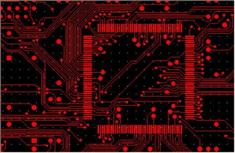
5. Overlapping or Touching Features
Overlapping or touching features can cause short circuits and other issues on the PCB. This mistake often occurs when designers do not adhere to the minimum clearance and spacing requirements specified by the PCB manufacturer.
To avoid this mistake:
– Familiarize yourself with the manufacturer’s design guidelines and requirements
– Use design rule checks (DRC) in your PCB design software to identify and fix overlapping or touching features
– Visually inspect your design for any potential overlaps or spacing issues
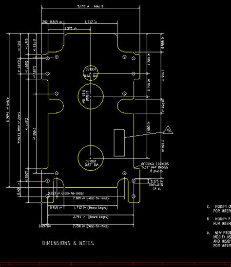
6. Incorrect Units and Dimensions
Using incorrect units or dimensions in your Gerber files can lead to manufacturing errors and delays. It is essential to ensure that all dimensions and units are consistent and correct throughout your design files.
To avoid this mistake:
– Confirm with your PCB manufacturer which units they prefer (e.g., inches or millimeters)
– Set the correct units in your PCB design software before creating your design
– Double-check all dimensions and units in your Gerber files before submitting them for manufacturing
7. Naming Conventions and File Extensions
Inconsistent or incorrect naming conventions and file extensions can cause confusion and delays in the manufacturing process. It is important to follow the manufacturer’s guidelines for naming your Gerber files and using the correct file extensions.
To avoid this mistake:
– Ask your PCB manufacturer for their preferred naming conventions and file extensions
– Use clear and descriptive names for your Gerber files (e.g., “ProjectName_TopCopper.gbr”)
– Verify that all file extensions are correct and match the manufacturer’s requirements
Gerber File Mistakes FAQ
Q: What happens if I forget to include an aperture list with my Gerber files?
A: If you forget to include an aperture list, the PCB manufacturer will not be able to accurately interpret your Gerber files. This can lead to manufacturing errors, delays, and increased costs. Always include an aperture list and ensure that it matches the features in your design.
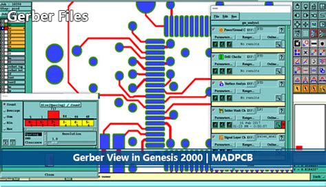
Q: How can I check if my Gerber files are correct before sending them to the manufacturer?
A: You can use a Gerber viewer to check your files for any errors or inconsistencies. A Gerber viewer allows you to visually inspect each layer, verify the aperture list, and ensure that all necessary information is included. Many PCB design software packages include built-in Gerber viewers, or you can use standalone viewers such as GerbView or ViewMate.
Q: What should I do if I’m unsure about the manufacturer’s design requirements?
A: If you are unsure about the manufacturer’s design requirements, the best course of action is to contact them directly. Most PCB manufacturers have a dedicated support team that can answer your questions and provide guidance on their specific requirements, such as preferred file formats, naming conventions, and design guidelines.
Q: Can I use different units for different layers in my Gerber files?
A: No, it is essential to maintain consistency in units throughout your Gerber files. Using different units for different layers can lead to manufacturing errors and delays. Confirm with your PCB manufacturer which units they prefer (e.g., inches or millimeters) and use those units consistently in your design and Gerber files.
Q: What are the consequences of submitting Gerber files with mistakes?
A: Submitting Gerber files with mistakes can lead to several consequences, including:
– Manufacturing errors and defects in the final PCB
– Delays in the production process
– Increased costs due to rework or redesign
– Damage to your reputation as a designer
To avoid these consequences, it is crucial to thoroughly check your Gerber files for mistakes before submitting them to the manufacturer and adhere to their design guidelines and requirements.
| Common Mistake | Consequence | How to Avoid |
|---|---|---|
| Missing or incorrect aperture list | Manufacturing errors | Include a correct aperture list |
| Incorrect drill file format | Confusion and delays | Use the manufacturer’s preferred format |
| Incomplete or missing layers | Non-functional PCB | Include all necessary layers |
| Incorrect layer polarity | PCB not functioning as intended | Confirm polarity with manufacturer |
| Overlapping or touching features | Short circuits | Follow manufacturer’s design guidelines |
| Incorrect units and dimensions | Manufacturing errors and delays | Use consistent and correct units |
| Inconsistent naming conventions and file extensions | Confusion and delays | Follow manufacturer’s guidelines |
By understanding and avoiding these common Gerber file mistakes, you can ensure a smooth and efficient PCB manufacturing process, saving time, money, and frustration. Always communicate with your PCB manufacturer, follow their guidelines, and thoroughly check your files before submitting them for production.
No responses yet