What are Nets in Altium Designer?
In Altium Designer, a net is an electrical connection between two or more component pins. Nets represent the wiring and connectivity in your schematic and PCB designs. Every pin on a component in your schematic must be connected to a net, whether it’s a signal net, power net, or ground net.
Nets play a critical role in defining the electrical behavior and functionality of your design. Some key characteristics of nets in Altium Designer include:
- Each net is identified by a unique name
- Nets can connect multiple pins across different components
- Nets transfer signals and power between components
- Nets have properties like width, color, and layer
- Nets are represented as copper traces, vias, and planes in the PCB layout
Managing and organizing nets is essential for creating accurate, high-quality schematic and PCB designs. This is where Altium Designer’s net highlighting features come in handy.
Benefits of Highlighting Nets
Highlighting nets in Altium Designer provides several advantages that simplify the schematic capture and PCB layout process:
- Visual Clarity
- Error Detection
- Design Navigation
- Documentation
Let’s explore each of these benefits in more detail.
Visual Clarity
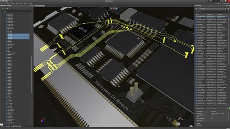
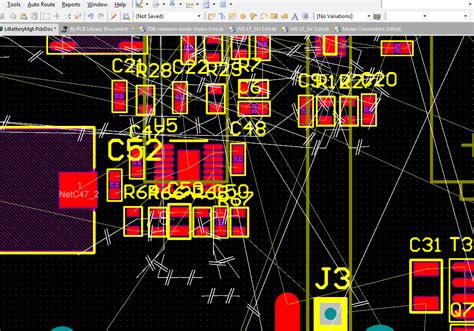
Highlighting nets allows you to visually trace the connections in your schematic and PCB with ease. With the click of a button, you can distinctly color the nets of interest while dimming the rest of the design. This provides an instant visual representation of how specific signals flow through your design.
For example, you can quickly identify which components are connected to a critical signal like a clock or chip select. Highlighting also helps you spot any unintended connections or short circuits that may otherwise go unnoticed in a complex design.
Error Detection
Catching design errors early is crucial for saving time and avoiding costly mistakes. Altium Designer’s real-time design rule checking (DRC) engine constantly monitors your schematic and layout for violations. When you highlight a net, the DRC will flag any errors associated with that net, such as:
- Unconnected pins
- Shorted pins
- Excessive net lengths
- Insufficient clearances
By focusing on one highlighted net at a time, you can systematically debug and resolve connectivity issues. This targeted approach is much more efficient than sifting through error markers scattered across a dense schematic or PCB.
Design Navigation
As designs grow in size and complexity, navigating between the schematic and PCB can become cumbersome. Fortunately, net highlighting creates a visual link that helps you quickly jump between corresponding parts of your design.
For instance, if you highlight a net in the schematic, Altium Designer will automatically highlight the same net in the PCB layout. This cross-probing feature works bidirectionally, allowing you to easily map nets from the schematic to the layout and vice versa.
Highlighting nets also simplifies navigating hierarchical designs. You can trace a net through multiple sheets in your schematic or multiple levels in your PCB stackup. This gives you a comprehensive view of how signals traverse your entire design.
Documentation
Clear and accurate documentation is essential for communicating design intent and facilitating future maintenance. Altium Designer’s net highlighting tools can enhance your documentation in several ways:
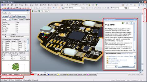
Annotated images – You can create snapshots of your schematic or PCB with specific nets highlighted to visually explain critical signal paths. These annotated images are ideal for datasheets, application notes, and design reviews.
Net reports – Altium Designer can generate detailed reports listing all the components and pins connected to a highlighted net. These reports provide a comprehensive view of net connectivity that complements graphical documentation.
Color-coded printouts – You can configure Altium Designer to print highlighted nets in different colors. Color-coded schematic and PCB printouts make it easier to trace signals and spot errors during manual reviews.
By leveraging highlighted nets in your documentation, you can create more informative and accessible design collateral. This not only benefits your own understanding of the design but also streamlines collaboration with teammates and stakeholders.
How to Highlight Nets in Altium Designer
Now that we’ve covered the benefits of net highlighting, let’s walk through the steps to highlight nets in Altium Designer. The process is straightforward and can be done in both the schematic and PCB editors.
Highlighting Nets in the Schematic Editor
- Open your schematic document in Altium Designer.
- Locate the net you want to highlight in the schematic.
- Double-click on the net to select it. Alternatively, you can click on the net and press the Tab key to select it.
- Right-click on the selected net and choose “Highlight Net” from the context menu. You can also use the keyboard shortcut “H” to highlight the net.
- The selected net will now be highlighted in a contrasting color, while the rest of the schematic will be dimmed.
- To unhighlight the net, right-click on it and choose “Unhighlight Net” from the context menu or press “H” again.
Highlighting Nets in the PCB Editor
- Open your PCB document in Altium Designer.
- Switch to the 2D Layout View if you’re not already in it.
- Locate the net you want to highlight on the PCB.
- Double-click on any object (trace, via, pad) that belongs to the net. Alternatively, you can click on the object and press the Tab key to select the entire net.
- Right-click on the selected net and choose “Highlight Net” from the context menu. You can also use the keyboard shortcut “H” to highlight the net.
- The selected net will now be highlighted in a contrasting color, while the rest of the PCB will be dimmed.
- To unhighlight the net, right-click on it and choose “Unhighlight Net” from the context menu or press “H” again.
Altium Designer also provides options to customize the appearance of highlighted nets. You can change the highlight color, contrast, and transparency to suit your preferences. These settings can be accessed from the “View” menu in both the schematic and PCB editors.

Real-World Applications
To better understand the value of net highlighting, let’s explore a couple of real-world applications where it can significantly simplify your design process.
Example 1: Debugging a Digital Circuit
Consider a scenario where you’re designing a complex digital circuit with multiple clock domains. During schematic capture, you realize that one of the clock nets is not behaving as expected. Tracing the clock net through a dense schematic can be time-consuming and error-prone.
This is where net highlighting comes to the rescue. By highlighting the problematic clock net, you can quickly identify all the components connected to it. This visual representation makes it easier to spot any missing or incorrect connections.
For instance, you may discover that a flip-flop is missing a clock input or that a clock buffer has its output shorted to ground. Highlighting the net allows you to pinpoint these errors and take corrective action.
Once you’ve resolved the issues in the schematic, you can cross-probe the clock net to the PCB layout. Highlighting the net in the layout helps you verify that the clock routing meets your design requirements, such as:
- Maintaining consistent trace widths and lengths
- Avoiding crosstalk with adjacent signals
- Providing adequate shielding and grounding
By leveraging net highlighting, you can efficiently debug your digital circuit and ensure its integrity from schematic to layout.
Example 2: Optimizing Power Delivery
Another common use case for net highlighting is optimizing power delivery in your PCB. Proper power distribution is critical for maintaining signal integrity and preventing voltage drops across your design.
Let’s say you’re designing a high-speed digital board with multiple power domains. Each domain requires a specific voltage level and current capacity. To optimize the power delivery network (PDN), you need to analyze the power nets and make appropriate design decisions.
Highlighting the power nets in your schematic allows you to:
- Identify the components connected to each power domain
- Verify that each component receives the correct voltage level
- Check for any missing or incorrect power connections
Once you’ve confirmed the schematic is accurate, you can highlight the power nets in the PCB layout. This helps you visualize how the power is distributed across the board and identify areas for improvement.
For example, you may notice that a particular power net has a long, thin trace that could cause excessive voltage drop. By highlighting the net, you can easily trace its path and modify the routing to use a wider trace or a copper pour.
Similarly, highlighting power nets can help you spot potential issues like:
- Insufficient via stitching between power planes
- Inadequate decoupling capacitor placement
- Crowded or congested areas that may cause thermal problems
By addressing these issues early in the design process, you can create a robust PDN that delivers clean, stable power to all your components. Net highlighting simplifies this optimization process by providing visual cues and facilitating cross-probing between the schematic and layout.
Best Practices for Using Net Highlighting
To get the most out of Altium Designer’s net highlighting features, consider the following best practices:
-
Use meaningful net names – Assign descriptive names to your nets that reflect their function or signal type. This makes it easier to identify and highlight specific nets in your design.
-
Highlight critical nets first – Prioritize highlighting nets that are critical to your design’s functionality, such as clock nets, reset lines, and power rails. These nets often have the most significant impact on performance and reliability.
-
Combine highlighting with filters – Use Altium Designer’s filtering options to selectively highlight nets based on criteria like name, layer, or object type. This can help you focus on specific subsets of nets relevant to your current task.
-
Document highlighted images – Capture screenshots of your schematic and PCB with important nets highlighted. Include these images in your design documentation to provide visual context and aid in future debugging or maintenance.
-
Collaborate using highlighted nets – When working in a team, use net highlighting to communicate design intent and review critical signal paths. Sharing highlighted images or design files helps ensure everyone is on the same page.
-
Iterate and refine – As your design evolves, periodically revisit and highlight nets to verify connectivity and catch any introduced errors. Net highlighting should be an integral part of your iterative design process.
By following these best practices, you can effectively leverage net highlighting to simplify your schematic and PCB designs in Altium Designer.
FAQ
-
Can I highlight multiple nets simultaneously in Altium Designer?
Yes, you can highlight multiple nets at once in Altium Designer. To do this, hold down the Ctrl key (Cmd on Mac) while selecting the desired nets. Then, right-click and choose “Highlight Nets” from the context menu. -
How do I change the color of highlighted nets?
To change the highlight color, go to the “View” menu in Altium Designer and select “Preferences.” In the preferences dialog, navigate to the “PCB Editor” or “Schematic Editor” section (depending on which editor you’re using) and look for the “Highlight Style” settings. Here, you can customize the color, contrast, and transparency of highlighted nets. -
Can I highlight nets in a multi-sheet schematic?
Yes, Altium Designer supports net highlighting across multiple schematic sheets. When you highlight a net on one sheet, Altium Designer will automatically highlight the corresponding net segments on all other sheets in the schematic document. -
Is there a way to quickly unhighlight all nets?
Yes, you can quickly unhighlight all nets by pressing the “U” key on your keyboard. This shortcut works in both the schematic and PCB editors. Alternatively, you can go to the “View” menu and select “Clear All Highlights.” -
Can I highlight nets based on their signal type or layer?
Yes, Altium Designer allows you to highlight nets based on various criteria. You can use the “Filter” panel in the PCB editor to create custom filters based on net attributes like signal type, layer, length, or name. Once you’ve defined your filter, you can highlight the matching nets with a single click.
By taking advantage of Altium Designer’s net highlighting features and following best practices, you can streamline your schematic and PCB design process. Highlighting nets provides visual clarity, aids in error detection, simplifies navigation, and enhances documentation. Whether you’re debugging a complex digital circuit or optimizing power delivery, net highlighting is a powerful tool in your design arsenal.
As you work on more advanced designs, consider exploring additional features in Altium Designer that complement net highlighting. For example, the “Find Similar Objects” command allows you to quickly select and highlight all objects that share common properties. This can be useful for identifying components with specific footprints or nets with matching widths.
Additionally, Altium Designer’s scripting and automation capabilities allow you to extend the functionality of net highlighting. You can write custom scripts to highlight nets based on complex criteria or to generate detailed reports on highlighted net properties.
In conclusion, net highlighting is an essential skill for any Altium Designer user. By mastering this feature, you can create more efficient, accurate, and visually intuitive schematic and PCB designs. Whether you’re a beginner or an experienced designer, investing time in learning and applying net highlighting techniques will pay dividends in your design productivity and quality.
No responses yet