Introduction to Ferrite Beads
Ferrite beads are passive electronic components that are widely used in electronic circuits to suppress high-frequency noise and electromagnetic interference (EMI). They are made of a magnetic ceramic material called ferrite, which has high permeability and resistivity. Ferrite beads are often used in power supply lines, data lines, and other signal paths to prevent unwanted high-frequency signals from propagating through the circuit.
How Ferrite Beads Work
Ferrite beads work by acting as a low-pass filter, allowing low-frequency signals to pass through while attenuating high-frequency signals. This is achieved through the combination of the bead’s inductance and resistance. At low frequencies, the bead acts as a simple conductor, allowing the signal to pass through with minimal attenuation. However, as the frequency increases, the impedance of the bead also increases, causing the high-frequency signals to be attenuated.
The equivalent circuit of a ferrite bead can be represented as a series combination of an inductor and a resistor. The inductance of the bead is determined by its geometry and the permeability of the ferrite material, while the resistance is determined by the conductivity of the ferrite and the winding of the wire through the bead.
Types of Ferrite Beads
There are several types of ferrite beads available, each with different characteristics and applications. Some common types include:
-
Surface Mount Device (SMD) Ferrite Beads: These are small, compact beads that are designed to be soldered directly onto a printed circuit board (PCB). They are available in various sizes and ratings, making them suitable for a wide range of applications.
-
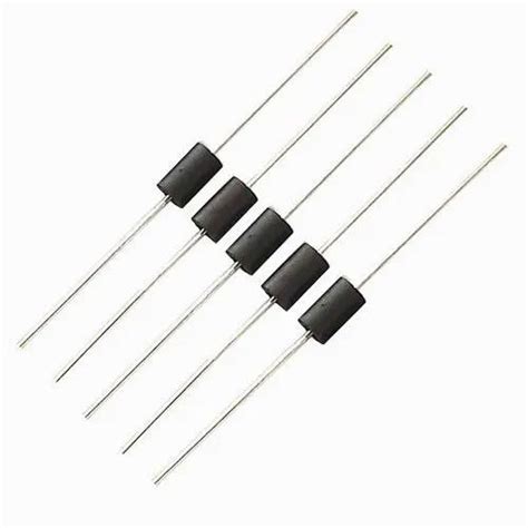
Through-Hole Ferrite Beads: These beads have wire leads that are inserted through holes in the PCB and soldered on the opposite side. They are larger than SMD beads and are often used in applications where higher current handling capacity is required.
-
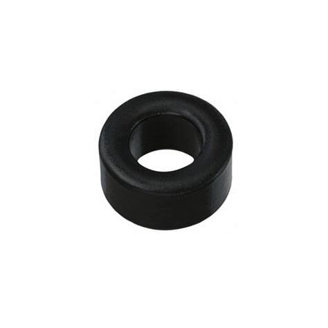
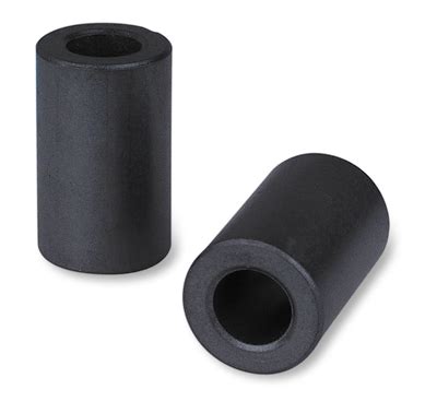
Ferrite Cores: These are larger ferrite components that are used to suppress EMI in cables and wires. They are available in various shapes, such as cylindrical, rectangular, and snap-on, and can be easily installed over the cable or wire.
Selecting the Right Ferrite Bead
When selecting a ferrite bead for a specific application, several factors need to be considered, including:
-
Impedance: The impedance of the bead should be chosen based on the frequency range of the noise that needs to be suppressed. Higher impedance beads are more effective at suppressing high-frequency noise, while lower impedance beads are better suited for lower frequency noise.
-
Current Rating: The maximum current that the bead can handle without saturating should be higher than the expected current in the circuit. Saturation of the bead can lead to a reduction in its impedance and a decrease in its effectiveness.
-
DC Resistance: The DC resistance of the bead should be low enough to minimize the voltage drop across the bead and the power dissipation in the circuit.
-
Size and Packaging: The size and packaging of the bead should be compatible with the circuit layout and the available space on the PCB.
Power Distribution Network (PDN) Simulation
Power Distribution Network (PDN) simulation is a crucial step in the design of electronic systems, particularly in high-speed digital circuits. The PDN is responsible for delivering clean and stable power to all the components in the system, and any issues in the PDN can lead to signal integrity problems, EMI, and reliability issues.
Why PDN Simulation is Important
PDN simulation helps designers analyze the performance of the power distribution network and identify potential issues before the circuit is fabricated. By simulating the PDN, designers can:
-
Verify that the PDN can deliver the required power to all the components in the system without excessive voltage drop or current density.
-
Identify resonances and impedance mismatches in the PDN that can lead to signal integrity issues and EMI.
-
Optimize the placement and sizing of decoupling capacitors and other components in the PDN to minimize impedance and ensure stable power delivery.
-
Analyze the impact of different PCB stackup and layout options on the PDN performance.
PDN Simulation Techniques
There are several techniques used for PDN simulation, each with its own advantages and limitations. Some common techniques include:
-
Lumped Element Modeling: This technique models the PDN as a network of lumped elements, such as resistors, inductors, and capacitors. Lumped element modeling is simple and fast, but it may not accurately capture the distributed effects in the PDN at high frequencies.
-
Distributed Modeling: This technique models the PDN as a distributed network, taking into account the transmission line effects and the frequency-dependent behavior of the materials. Distributed modeling is more accurate than lumped element modeling, but it is also more complex and computationally intensive.
-
Finite Element Analysis (FEA): This technique uses numerical methods to solve the electromagnetic field equations in the PDN. FEA can accurately model complex geometries and material properties, but it requires significant computational resources and expertise.
-
Hybrid Modeling: This technique combines lumped element and distributed modeling to achieve a balance between accuracy and complexity. Hybrid modeling uses lumped elements to model the low-frequency behavior of the PDN and distributed elements to model the high-frequency behavior.
PDN Simulation Tools
There are several commercial and open-source tools available for PDN simulation, each with its own features and capabilities. Some popular tools include:
-
Ansys SIwave: A comprehensive tool for modeling and simulating PDNs in high-speed electronic systems. SIwave supports lumped element, distributed, and hybrid modeling, and includes a library of pre-defined components and materials.
-
Cadence Sigrity: A suite of tools for modeling and analyzing PDNs in PCBs and packages. Sigrity includes tools for DC and AC analysis, decoupling capacitor optimization, and electro-magnetic interference (EMI) analysis.
-
Mentor Graphics HyperLynx: A tool for modeling and simulating PDNs in PCBs and packages. HyperLynx includes tools for DC and AC analysis, decoupling capacitor optimization, and signal integrity analysis.
-
Altium Designer: A PCB design tool that includes a built-in PDN analyzer for modeling and simulating PDNs. The PDN analyzer supports lumped element and distributed modeling, and includes a library of pre-defined components and materials.
Transfer Impedance
Transfer impedance is a key parameter in the design of PDNs, particularly in the context of ferrite beads. Transfer impedance is a measure of the coupling between the input and output of a device, and it determines the effectiveness of the device in suppressing noise and EMI.
Definition of Transfer Impedance
Transfer impedance is defined as the ratio of the voltage induced on the output of a device to the current flowing through the input of the device. In the context of ferrite beads, transfer impedance is a measure of the bead’s ability to suppress high-frequency noise and EMI.
The transfer impedance of a ferrite bead is typically specified in terms of its magnitude and phase as a function of frequency. The magnitude of the transfer impedance determines the amount of attenuation provided by the bead, while the phase determines the frequency range over which the attenuation occurs.
Measuring Transfer Impedance
Transfer impedance can be measured using a variety of techniques, including:
-
Network Analyzer: A network analyzer can be used to measure the S-parameters of the ferrite bead, which can then be used to calculate the transfer impedance. This technique is accurate and versatile, but it requires expensive equipment and expertise.
-
Impedance Analyzer: An impedance analyzer can be used to measure the impedance of the ferrite bead directly. This technique is simpler and less expensive than using a network analyzer, but it may not provide as much information about the frequency-dependent behavior of the bead.
-
Time Domain Reflectometry (TDR): TDR can be used to measure the impedance of the ferrite bead in the time domain, which can then be converted to the frequency domain using Fourier analysis. This technique is fast and easy to use, but it may not provide as much accuracy as other techniques.
Simulating Transfer Impedance
Transfer impedance can also be simulated using PDN simulation tools. By modeling the ferrite bead as a lumped element or distributed network, designers can simulate the transfer impedance of the bead and analyze its impact on the PDN performance.
To simulate the transfer impedance of a ferrite bead, designers need to:
-
Create a model of the ferrite bead using lumped elements or distributed elements, based on the bead’s geometry and material properties.
-
Add the ferrite bead model to the PDN simulation, either as a discrete component or as part of the PCB stackup.
-
Simulate the PDN with and without the ferrite bead, and compare the results to determine the impact of the bead on the PDN performance.
-
Optimize the placement and value of the ferrite bead to achieve the desired transfer impedance and PDN performance.

Conclusion
Ferrite beads are a crucial component in the design of high-speed electronic systems, particularly in the context of power distribution networks (PDNs). By suppressing high-frequency noise and EMI, ferrite beads can help ensure the stability and reliability of the PDN and the overall system.
PDN simulation is a powerful tool for analyzing the performance of ferrite beads and optimizing their placement and value in the PDN. By simulating the transfer impedance of the ferrite bead and its impact on the PDN, designers can identify potential issues and optimize the PDN design for maximum performance and reliability.
When selecting ferrite beads for a specific application, designers need to consider factors such as impedance, current rating, DC resistance, and size and packaging. By carefully selecting the right ferrite bead and optimizing its placement in the PDN, designers can achieve the best possible performance and reliability in their electronic systems.
FAQ
-
What is the purpose of using ferrite beads in electronic circuits?
Ferrite beads are used in electronic circuits to suppress high-frequency noise and electromagnetic interference (EMI). They act as low-pass filters, allowing low-frequency signals to pass through while attenuating high-frequency signals. -
How do I select the right ferrite bead for my application?
When selecting a ferrite bead, consider factors such as the impedance, current rating, DC resistance, and size and packaging. The impedance should be chosen based on the frequency range of the noise that needs to be suppressed, while the current rating should be higher than the expected current in the circuit. The DC resistance should be low enough to minimize voltage drop and power dissipation, and the size and packaging should be compatible with the circuit layout and available space. -
What is PDN simulation and why is it important?
Power Distribution Network (PDN) simulation is the process of analyzing the performance of the power distribution network in an electronic system. It helps designers verify that the PDN can deliver the required power to all components without excessive voltage drop or current density, identify resonances and impedance mismatches that can lead to signal integrity issues and EMI, and optimize the placement and sizing of decoupling capacitors and other components in the PDN. -
What is transfer impedance and how is it related to ferrite beads?
Transfer impedance is a measure of the coupling between the input and output of a device, and it determines the effectiveness of the device in suppressing noise and EMI. In the context of ferrite beads, transfer impedance is a measure of the bead’s ability to suppress high-frequency noise and EMI. The transfer impedance of a ferrite bead is typically specified in terms of its magnitude and phase as a function of frequency. -
How can I simulate the transfer impedance of a ferrite bead in my PDN design?
To simulate the transfer impedance of a ferrite bead in a PDN design, you need to create a model of the ferrite bead using lumped elements or distributed elements, based on the bead’s geometry and material properties. Then, add the ferrite bead model to the PDN simulation, either as a discrete component or as part of the PCB stackup. Simulate the PDN with and without the ferrite bead, and compare the results to determine the impact of the bead on the PDN performance. Finally, optimize the placement and value of the ferrite bead to achieve the desired transfer impedance and PDN performance.
No responses yet