Introduction to Annular rings in PCB Design
Annular rings are an essential aspect of printed circuit board (PCB) design, particularly in multilayer boards. These rings, which surround the drilled holes in a PCB, play a crucial role in ensuring the reliability and functionality of the final product. In this article, we will explore the importance of annular rings, their design considerations, and how to stay within tolerances when designing multilayer PCBs.
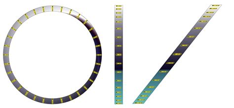
What are Annular Rings?
Annular rings, also known as pad rings or land rings, are the circular copper areas that surround the drilled holes in a PCB. These rings provide a connection between the component leads or pins and the copper traces on the PCB layers. The primary purpose of annular rings is to ensure a reliable electrical and mechanical connection between the components and the board.
The Importance of Annular Rings in PCB Design
Annular rings serve several critical functions in PCB design:
-
Electrical Connectivity: Annular rings provide a conductive path between the component leads and the copper traces on the PCB layers, ensuring proper electrical connectivity.
-
Mechanical Strength: The annular ring helps to distribute the mechanical stress around the hole, preventing the copper from lifting or separating from the board during the soldering process or due to thermal expansion and contraction.
-
Manufacturing Tolerance: Annular rings provide a margin of error for the drilling process, accommodating slight misalignments between the drilled hole and the intended location of the component lead.
-
Current Carrying Capacity: The size of the annular ring affects the current carrying capacity of the connection. Larger annular rings can carry more current, which is essential for power-intensive components.
Designing Annular Rings for Multilayer PCBs
When designing annular rings for multilayer PCBs, several factors must be considered to ensure the best performance and reliability of the final product.
Annular Ring Size
The size of the annular ring is a critical factor in PCB design. The ring must be large enough to provide a reliable connection and accommodate manufacturing tolerances, but not so large that it unnecessarily consumes board space or creates signal integrity issues.
The minimum annular ring size is typically determined by the PCB manufacturer’s capabilities and the specific requirements of the design. As a general rule, the minimum annular ring size should be at least 0.15mm (6 mil) larger than the drilled hole diameter.
| Drilled Hole Diameter | Minimum Annular Ring Size |
|---|---|
| 0.2mm (8 mil) | 0.35mm (14 mil) |
| 0.3mm (12 mil) | 0.45mm (18 mil) |
| 0.4mm (16 mil) | 0.55mm (22 mil) |
| 0.5mm (20 mil) | 0.65mm (26 mil) |
Pad stack design
In multilayer PCBs, the pad stack design is crucial for ensuring proper connectivity between layers. The pad stack refers to the arrangement of the annular rings and drilled holes through the various layers of the board.
When designing the pad stack, consider the following:
-
Consistent Annular Ring Size: Maintain a consistent annular ring size across all layers of the pad stack to ensure uniform current carrying capacity and mechanical strength.
-
Thermal Relief: In power or ground planes, use thermal relief connections to reduce the heat sinking effect of the plane and improve solderability. Thermal relief connections are small traces that connect the annular ring to the plane, allowing heat to dissipate during soldering.
-
Via Placement: When placing vias in the pad stack, ensure that they do not intersect with the component lead or pin. This can cause manufacturing issues and compromise the reliability of the connection.
Clearance and Creepage Distance
Clearance and creepage distance are essential considerations when designing annular rings for multilayer PCBs. Clearance is the shortest distance between two conductive elements through air, while creepage is the shortest distance along the surface of the insulating material between two conductive elements.
To ensure proper insulation and prevent electrical shorts, maintain sufficient clearance and creepage distance between annular rings and adjacent conductive elements. The specific requirements for clearance and creepage distance depend on the voltage, pollution degree, and insulating material of the PCB.
| Voltage | Minimum Clearance | Minimum Creepage |
|---|---|---|
| ≤ 50V | 0.1mm (4 mil) | 0.2mm (8 mil) |
| ≤ 100V | 0.2mm (8 mil) | 0.4mm (16 mil) |
| ≤ 150V | 0.3mm (12 mil) | 0.6mm (24 mil) |
| ≤ 300V | 0.5mm (20 mil) | 1.0mm (40 mil) |

Manufacturing Considerations for Annular Rings
When designing annular rings for multilayer PCBs, it is essential to consider the manufacturing process and its limitations. Collaborating with your PCB manufacturer early in the design process can help you avoid potential issues and ensure the best possible results.
Drilling Accuracy
The accuracy of the drilling process is a critical factor in annular ring design. Misaligned or oversized holes can compromise the integrity of the annular ring and lead to manufacturing defects.
To accommodate drilling tolerances, design your annular rings with sufficient size to allow for slight misalignments. Work with your PCB manufacturer to understand their drilling capabilities and tolerances, and design your annular rings accordingly.
Plating and Finishing
The plating and finishing processes can also affect the performance and reliability of annular rings. Ensure that the plating thickness is sufficient to provide a reliable connection and withstand the mechanical stresses of the soldering process.
When specifying the finishing material, consider the compatibility with the soldering process and the environmental requirements of the final product. Common finishing materials include hot air solder leveling (HASL), immersion silver, immersion tin, and electroless nickel immersion gold (ENIG).
Solder Mask and Solder Paste
The solder mask and solder paste application processes can impact the quality of the annular ring connection. Ensure that the solder mask aperture is correctly aligned with the annular ring and provides adequate clearance for the soldering process.
When applying solder paste, use a stencil with the appropriate thickness and aperture size to ensure a consistent and sufficient solder volume. Insufficient solder paste can result in weak connections, while excessive solder paste can cause bridging or other soldering defects.

Best Practices for Annular Ring Design
To ensure the best performance and reliability of your multilayer PCB, follow these best practices when designing annular rings:
- Use appropriate annular ring sizes based on the drilled hole diameter and manufacturing capabilities.
- Maintain consistent annular ring sizes across all layers of the pad stack.
- Use thermal relief connections in power and ground planes to improve solderability.
- Ensure sufficient clearance and creepage distance between annular rings and adjacent conductive elements.
- Collaborate with your PCB manufacturer early in the design process to understand their capabilities and limitations.
- Design annular rings with sufficient size to accommodate drilling tolerances.
- Specify appropriate plating and finishing materials based on the soldering process and environmental requirements.
- Ensure proper alignment and clearance of the solder mask aperture with the annular ring.
- Use appropriate solder paste stencil thickness and aperture size for consistent and sufficient solder volume.
- Conduct thorough design reviews and manufacturability assessments to identify and address potential issues early in the design process.

Frequently Asked Questions (FAQ)
-
What is the purpose of annular rings in PCB design?
Annular rings provide a reliable electrical and mechanical connection between component leads or pins and the copper traces on the PCB layers. They also accommodate manufacturing tolerances and help distribute mechanical stress around the drilled hole. -
How do I determine the minimum annular ring size for my design?
The minimum annular ring size is typically determined by the PCB manufacturer’s capabilities and the specific requirements of the design. As a general rule, the minimum annular ring size should be at least 0.15mm (6 mil) larger than the drilled hole diameter. -
What is the importance of pad stack design in multilayer PCBs?
Pad stack design ensures proper connectivity between layers in a multilayer PCB. It involves maintaining consistent annular ring sizes, using thermal relief connections in power and ground planes, and ensuring proper via placement to avoid intersecting with component leads or pins. -
How do clearance and creepage distance affect annular ring design?
Clearance and creepage distance are essential for ensuring proper insulation and preventing electrical shorts between annular rings and adjacent conductive elements. The specific requirements depend on the voltage, pollution degree, and insulating material of the PCB. -
What are some best practices for designing annular rings in multilayer PCBs?
Some best practices include using appropriate annular ring sizes, maintaining consistent sizes across pad stack layers, using thermal relief connections, ensuring sufficient clearance and creepage distance, collaborating with the PCB manufacturer, accommodating drilling tolerances, specifying appropriate plating and finishing materials, ensuring proper solder mask alignment, and using appropriate solder paste stencil thickness and aperture size.
Conclusion
Annular rings are a critical aspect of multilayer PCB design, ensuring reliable electrical and mechanical connections between components and the board. By understanding the importance of annular rings, designing them with consideration for manufacturing processes, and following best practices, you can create high-quality, reliable PCBs that meet your specific requirements.
Remember to collaborate with your PCB manufacturer throughout the design process to ensure that your annular ring design is compatible with their capabilities and tolerances. By staying within these tolerances and adhering to industry standards, you can minimize the risk of manufacturing defects and ensure the best possible performance of your multilayer PCB.
No responses yet