PCB Design Market Size and Growth
The global printed circuit board (PCB) market size was valued at USD 61.5 billion in 2020 and is projected to reach USD 75.7 billion by 2028, growing at a CAGR of 3.1% from 2021 to 2028.
| Year | Market Size (USD Billion) |
|---|---|
| 2020 | 61.5 |
| 2021 | 63.4 |
| 2022 | 65.4 |
| 2023 | 67.4 |
| 2024 | 69.5 |
| 2025 | 71.6 |
| 2026 | 73.8 |
| 2027 | 76.0 |
| 2028 | 75.7 |
The growth of the PCB market is driven by increasing demand for consumer electronics, automotive electronics, and the adoption of advanced technologies like 5G, IoT, and AI.
Consumer Electronics Dominates PCB Demand
Consumer electronics, including smartphones, tablets, laptops, and wearables, account for the largest share of PCB demand. In 2020, this segment held a market share of 29.5%.
| Application | Market Share (2020) |
|---|---|
| Consumer Electronics | 29.5% |
| Communication | 16.2% |
| Computer/Peripherals | 14.8% |
| Automotive | 11.3% |
| Industrial Electronics | 9.6% |
| Military/Aerospace | 6.4% |
| Medical | 4.1% |
| Others | 8.1% |
As consumer demand for electronics continues to grow, especially in emerging markets, the PCB industry will see sustained growth in this segment.
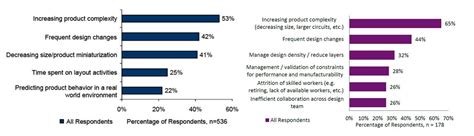
PCB Layer Count Distribution
The number of layers in a PCB is a key factor in its complexity and cost. Here’s how PCB designs are distributed by layer count:
| Number of Layers | Percentage of Designs |
|---|---|
| 1-2 | 25% |
| 4 | 50% |
| 6 | 15% |
| 8 | 7% |
| 10+ | 3% |
As you can see, 4-layer PCBs are the most common, accounting for half of all designs. Single and double-sided boards make up a quarter of designs, while 6-layer and above are less frequent due to their higher complexity and cost.
High Density Interconnect (HDI) PCBs on the Rise
HDI PCBs, which feature smaller vias, finer traces, and higher layer counts, are becoming increasingly popular to accommodate the miniaturization of electronic devices. The global HDI PCB market is projected to grow at a CAGR of 11.2% from 2021 to 2026, reaching USD 22.7 billion by 2026.

PCB Material Breakdown
FR-4 is the most widely used PCB material, thanks to its good mechanical and electrical properties, as well as its affordability. Here’s a breakdown of common PCB materials:
| Material | Percentage of Use |
|---|---|
| FR-4 | 70% |
| Polyimide | 10% |
| High-Tg FR-4 | 8% |
| Rogers (High Freq) | 5% |
| Flexible PCBs | 4% |
| Others | 3% |
While FR-4 dominates, specialized materials like polyimide and Rogers are used for applications that require higher temperature resistance or RF performance.

PCB Manufacturing Regional Distribution
China is the world’s largest PCB manufacturing hub, accounting for over half of global production. Here’s how PCB manufacturing is distributed globally:
| Region | Share of Global Production |
|---|---|
| China | 52.4% |
| Taiwan | 12.6% |
| South Korea | 8.2% |
| Japan | 7.1% |
| North America | 4.8% |
| Europe | 3.5% |
| Others | 11.4% |
While China leads in volume, other regions like Taiwan, South Korea, and Japan are known for their high-end PCB manufacturing capabilities.
Reshoring Trends in PCB Manufacturing
Despite China’s dominance, there’s a growing trend of PCB manufacturing reshoring, especially in North America and Europe. This is driven by factors such as:
- Supply chain disruptions during the COVID-19 pandemic
- Geopolitical tensions and trade disputes
- Increasing focus on supply chain resilience and diversification
- Growing demand for quick-turn prototyping and low-volume production
While reshoring is unlikely to significantly dent China’s market share in the short term, it’s an important trend to watch for in the coming years.
PCB Design Software Market Share
There are several popular PCB design software packages on the market, each with its own strengths and user base. Here’s a breakdown of the market share for top PCB design software:
| Software | Market Share |
|---|---|
| Altium | 25% |
| Cadence | 20% |
| Mentor | 18% |
| Zuken | 12% |
| Eagle | 10% |
| KiCad | 8% |
| Others | 7% |
Altium and Cadence lead the pack, with Mentor and Zuken also holding significant shares. Eagle and KiCad are popular choices for hobbyists and small businesses due to their lower cost and open-source nature.
Cloud-Based PCB Design Tools Gaining Traction
In recent years, there’s been a growing trend towards cloud-based PCB design tools. These tools offer advantages like:
- Accessibility from anywhere with an internet connection
- Easier collaboration between team members
- Scalable computing resources
- Automatic updates and maintenance
Some examples of cloud-based PCB design tools include Altium 365, Autodesk Fusion 360, and EasyEDA. While still a small portion of the overall market, cloud-based tools are expected to gain market share in the coming years.
PCB Failure Modes and Reliability
Ensuring the reliability of PCBs is crucial, especially in critical applications like medical devices, aerospace, and automotive. Here are some common PCB failure modes and their relative frequencies:
| Failure Mode | Relative Frequency |
|---|---|
| Solder joint failures | 30% |
| Component failures | 25% |
| Trace/via failures | 20% |
| PCB delamination/cracking | 10% |
| Environmental factors (moisture, heat, etc.) | 10% |
| Others | 5% |
To mitigate these failures, PCB designers can employ techniques like:
- Proper component selection and placement
- Robust solder joint design
- Adequate trace width and spacing
- Using appropriate PCB materials and surface finishes
- Incorporating design for manufacturing (DFM) and design for reliability (DFR) principles
By understanding common failure modes and designing with reliability in mind, PCB designers can create products that stand the test of time.
FAQ
Q1: What’s driving the growth of the PCB market?
A1: The growth of the PCB market is primarily driven by increasing demand for consumer electronics, automotive electronics, and the adoption of advanced technologies like 5G, IoT, and AI.
Q2: Why are 4-layer PCBs so common?
A2: 4-layer PCBs strike a good balance between complexity and cost. They offer more routing space and better signal integrity than 1-2 layer boards, while being less expensive and easier to manufacture than higher layer count boards.
Q3: What are the advantages of HDI PCBs?
A3: HDI (High Density Interconnect) PCBs offer several advantages, including smaller form factors, higher component density, improved signal integrity, and better thermal management. They are increasingly used in miniaturized electronic devices like smartphones and wearables.
Q4: Why is China the world’s largest PCB manufacturing hub?
A4: China has a well-established electronics manufacturing ecosystem, with a large pool of skilled labor, extensive supply chain networks, and government support for the industry. This has allowed China to achieve economies of scale and offer competitive pricing for PCB manufacturing.
Q5: What are the benefits of using cloud-based PCB design tools?
A5: Cloud-based PCB design tools offer advantages like accessibility from anywhere, easier collaboration between team members, scalable computing resources, and automatic updates and maintenance. They are gaining popularity, especially among remote teams and small businesses.
By staying informed about these PCB design stats and trends, you’ll be well-equipped to make smart design decisions and impress your colleagues with your industry knowledge. So go ahead and wow them around the water cooler!
No responses yet