Introduction to 3D-Printed-PCBs
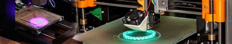
In recent years, the advent of 3D printing technology has revolutionized various industries, including electronics manufacturing. One of the most exciting developments in this field is the ability to 3D print electronic boards, also known as 3D-printed-PCBs (Printed Circuit Boards). This innovative approach offers numerous advantages over traditional PCB fabrication methods, such as rapid prototyping, cost-effectiveness, and design flexibility.
What are 3D-Printed-PCBs?
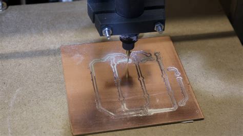
3D-printed-PCBs are electronic circuit boards that are manufactured using additive manufacturing techniques, specifically 3D printing technology. Unlike conventional PCB fabrication, which involves subtractive processes like etching and drilling, 3D printing builds the circuit board layer by layer, depositing conductive and insulating materials precisely where needed.
Advantages of 3D-Printed-PCBs
- Rapid Prototyping: 3D printing allows for quick and efficient prototyping of electronic boards, reducing the time and cost associated with traditional PCB fabrication methods.
- Design Flexibility: With 3D printing, designers have greater freedom to create complex geometries and incorporate unique features that may be challenging or impossible with conventional PCB manufacturing.
- Cost-Effectiveness: For low-volume production or prototyping, 3D printing can be more cost-effective than traditional PCB fabrication, as it eliminates the need for expensive tooling and setup costs.
- Customization: 3D-printed-PCBs enable easy customization of electronic boards, allowing designers to tailor the board’s shape, size, and functionality to specific application requirements.
3D Printing Technologies for PCBs
Several 3D printing technologies have been adapted for the fabrication of electronic boards, each with its own advantages and limitations.
Fused Deposition Modeling (FDM)
FDM is one of the most common and affordable 3D printing technologies. In the context of 3D-printed-PCBs, FDM printers are used to deposit conductive filaments, such as those containing copper or silver particles, onto a substrate to create the desired circuit pattern. The process is relatively simple and accessible, making it suitable for hobbyists and small-scale prototyping.
Advantages of FDM for 3D-Printed-PCBs
- Low cost and wide availability of FDM printers
- Ease of use and minimal setup requirements
- Compatibility with a range of conductive filaments
Limitations of FDM for 3D-Printed-PCBs
- Lower resolution and accuracy compared to other 3D printing technologies
- Limited conductivity of FDM-printed traces
- Potential for layer adhesion issues and warping
Stereolithography (SLA) and Digital Light Processing (DLP)
SLA and DLP are resin-based 3D printing technologies that use light to selectively cure and harden photopolymer resins layer by layer. For 3D-printed-PCBs, these technologies can be used to create high-resolution, smooth-surfaced circuit boards with embedded conductive traces.
Advantages of SLA/DLP for 3D-Printed-PCBs
- High resolution and accuracy, enabling the creation of fine-pitch traces
- Smooth surface finish, reducing the need for post-processing
- Ability to create complex geometries and intricate designs
Limitations of SLA/DLP for 3D-Printed-PCBs
- Higher cost compared to FDM
- Requires specialized resins and post-processing steps
- Limited material options for conductive traces
Inkjet Printing
Inkjet printing is a highly precise and versatile technology that has been adapted for the fabrication of 3D-printed-PCBs. This method involves the selective deposition of conductive inks onto a substrate using a high-resolution inkjet printhead. The conductive ink, typically containing silver or copper nanoparticles, is then sintered or cured to form the desired circuit pattern.
Advantages of Inkjet Printing for 3D-Printed-PCBs
- High precision and resolution, enabling the creation of fine-pitch traces
- Ability to deposit multiple materials, allowing for the integration of passive components
- Scalability and potential for high-volume production
Limitations of Inkjet Printing for 3D-Printed-PCBs
- Requires specialized inkjet printers and conductive inks
- Potential for nozzle clogging and inconsistent ink deposition
- Higher cost compared to FDM
Design Considerations for 3D-Printed-PCBs
When designing 3D-printed-PCBs, several key factors must be taken into account to ensure optimal performance and manufacturability.
Material Selection
Choosing the right materials for both the substrate and conductive traces is crucial for the success of a 3D-printed-PCB. The substrate material should have good mechanical properties, thermal stability, and dielectric characteristics. Common substrate materials include:
- Polylactic Acid (PLA)
- Acrylonitrile Butadiene Styrene (ABS)
- Polyethylene Terephthalate Glycol (PETG)
- Photopolymer resins (for SLA/DLP)
For conductive traces, the material should have high electrical conductivity, good adhesion to the substrate, and compatibility with the chosen 3D printing technology. Popular choices include:
- Conductive filaments (for FDM)
- Conductive resins (for SLA/DLP)
- Silver or copper nanoparticle inks (for inkjet printing)
Trace Width and Spacing
The minimum trace width and spacing achievable with 3D-printed-PCBs depend on the resolution and accuracy of the chosen 3D printing technology. Designers should consider the limitations of their selected method when defining trace dimensions to ensure manufacturability and reliable electrical performance.
| 3D Printing Technology | Typical Minimum Trace Width | Typical Minimum Trace Spacing |
|---|---|---|
| FDM | 0.5 mm | 0.5 mm |
| SLA/DLP | 0.1 mm | 0.1 mm |
| Inkjet Printing | 0.05 mm | 0.05 mm |
Layer Thickness and Orientation
The layer thickness and orientation of a 3D-printed-PCB can significantly impact its mechanical and electrical properties. Thinner layers generally result in smoother surfaces and higher resolution but may increase printing time. Orienting the PCB design to minimize the number of overhanging features and support structures can improve print quality and reduce post-processing requirements.
Post-Processing
After 3D printing, most PCBs require some form of post-processing to enhance their electrical and mechanical properties. This may include:
- Cleaning and removal of support structures
- Sanding or polishing to improve surface finish
- Sintering or curing of conductive traces to increase conductivity
- Applying protective coatings or encapsulants to improve durability

Applications of 3D-Printed-PCBs
3D-printed-PCBs have found applications in various fields, ranging from hobbyist projects to advanced research and development.
Rapid Prototyping and Proof-of-Concept
One of the most common applications of 3D-printed-PCBs is in rapid prototyping and proof-of-concept development. The ability to quickly and cost-effectively fabricate functional circuit boards enables designers and engineers to test and iterate their designs without the need for expensive and time-consuming traditional PCB fabrication methods.
Customized and Low-Volume Production
3D-printed-PCBs are particularly well-suited for customized and low-volume production runs, where the cost and lead time of conventional PCB manufacturing may be prohibitive. This makes 3D printing an attractive option for niche applications, specialized sensors, and one-off designs.
Wearable Electronics and Flexible Circuits
The design flexibility offered by 3D printing allows for the creation of non-planar and flexible circuit boards, which are essential for wearable electronics and other applications requiring conformable or stretchable circuits. By using flexible substrate materials and conductive traces, 3D-printed-PCBs can be integrated into clothing, accessories, and medical devices.
Educational and Hobbyist Use
3D-printed-PCBs have gained popularity among educators, students, and hobbyists as a means to learn about electronics and circuit design. The accessibility and affordability of 3D printing technology have made it possible for individuals to create their own custom circuit boards without the need for expensive equipment or extensive technical knowledge.
Challenges and Future Developments
Despite the numerous advantages of 3D-printed-PCBs, there are still challenges and limitations that need to be addressed for widespread adoption.
Conductivity and Durability
One of the main challenges facing 3D-printed-PCBs is the relatively low conductivity of printed traces compared to traditional copper traces. Researchers are continuously developing new conductive materials and post-processing techniques to improve the electrical performance of 3D-printed circuits. Additionally, the durability and long-term reliability of 3D-printed-PCBs need to be further investigated and improved.
Integration of Components
Currently, most 3D-printed-PCBs require the manual placement and soldering of electronic components after the printing process. Efforts are being made to develop methods for the direct integration of components during the 3D printing process, such as the use of pick-and-place systems or the embedding of components within the substrate material.
Multi-Material Printing
The ability to print multiple materials simultaneously, including conductive, insulating, and dielectric materials, would greatly expand the capabilities of 3D-printed-PCBs. Research is ongoing to develop multi-material 3D printing systems that can deposit a wide range of functional materials with high precision and resolution.
Standardization and Quality Control
As 3D-printed-PCBs gain more widespread adoption, there will be a growing need for standardization and quality control measures to ensure consistent performance and reliability. The development of industry standards, testing protocols, and certification processes will be essential for the successful integration of 3D-printed-PCBs into mainstream electronics manufacturing.
Frequently Asked Questions (FAQ)
-
What is the minimum feature size achievable with 3D-printed-PCBs?
The minimum feature size, such as trace width and spacing, depends on the 3D printing technology used. FDM typically achieves a minimum feature size of around 0.5 mm, while SLA/DLP and inkjet printing can produce features as small as 0.1 mm and 0.05 mm, respectively. -
Can 3D-printed-PCBs be used for high-frequency applications?
Currently, 3D-printed-PCBs are mostly suitable for low-frequency applications due to the limitations in conductivity and surface finish. However, ongoing research and development efforts aim to improve the performance of 3D-printed-PCBs for high-frequency applications by using advanced materials and processing techniques. -
Are 3D-printed-PCBs suitable for mass production?
3D-printed-PCBs are primarily used for prototyping, low-volume production, and customized applications. While some 3D printing technologies, such as inkjet printing, show potential for scalability, traditional PCB manufacturing methods are still more cost-effective and efficient for mass production. -
Can 3D-printed-PCBs be made with multiple layers?
Yes, 3D-printed-PCBs can be fabricated with multiple layers by using techniques such as multi-material printing or the stacking and bonding of individually printed layers. However, the complexity and reliability of multi-layer 3D-printed-PCBs are still areas of active research and development. -
How do the costs of 3D-printed-PCBs compare to traditional PCB manufacturing?
The cost-effectiveness of 3D-printed-PCBs depends on the specific application, volume, and design complexity. For low-volume production and prototyping, 3D printing can be more cost-effective than traditional PCB manufacturing, as it eliminates the need for expensive tooling and setup costs. However, for high-volume production, conventional PCB fabrication methods are generally more economical.
Conclusion
3D-printed-PCBs represent an exciting development in electronics manufacturing, offering numerous advantages such as rapid prototyping, design flexibility, and cost-effectiveness for low-volume production. As 3D printing technologies continue to advance, the capabilities and applications of 3D-printed-PCBs are expected to expand, enabling new possibilities in customized electronics, wearable devices, and beyond.
However, challenges related to conductivity, durability, component integration, and standardization must be addressed to fully realize the potential of 3D-printed-PCBs. Ongoing research and development efforts in materials science, multi-material printing, and post-processing techniques are crucial for overcoming these limitations and unlocking the full potential of this innovative technology.
As the field of 3D-printed-PCBs continues to evolve, it is poised to play an increasingly important role in shaping the future of electronics manufacturing, offering unparalleled flexibility, customization, and accessibility for designers, engineers, and enthusiasts alike.
No responses yet