Introduction
Designing a circuit board can be a complex and time-consuming process, especially for beginners. However, with the right tools and techniques, it can be made much easier. In this article, we will walk you through 10 easy steps to comprehensively design a circuit board using Altium Designer, one of the most popular PCB design software tools available.
Step 1: Create a New Project
To begin designing your circuit board, you first need to create a new project in Altium Designer. Here’s how:
- Open Altium Designer and click on “File” in the top menu bar.
- Select “New” and then “Project”.
- Choose the type of project you want to create (e.g., PCB Project) and give it a name.
- Click “OK” to create the project.

Step 2: Create a Schematic
The next step is to create a schematic of your circuit. A schematic is a graphical representation of the electrical connections in your circuit. Here’s how to create a schematic in Altium Designer:
- In the Projects panel, right-click on your project and select “Add New to Project”.
- Choose “Schematic” and give it a name.
- Double-click on the new schematic to open it.
- Use the components library to add the necessary components to your schematic.
- Use the wiring tool to connect the components according to your circuit design.

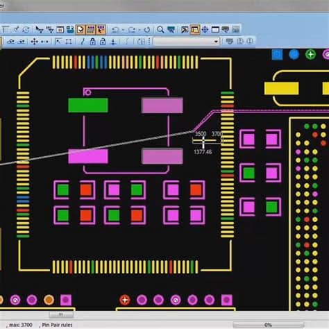
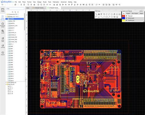
Step 3: Create a PCB Layout
Once you have created your schematic, you need to create a PCB layout. A PCB layout is a physical representation of your circuit, showing where each component will be placed on the board and how they will be connected. Here’s how to create a PCB layout in Altium Designer:
- In the Projects panel, right-click on your project and select “Add New to Project”.
- Choose “PCB” and give it a name.
- Double-click on the new PCB to open it.
- Use the “Import Changes” feature to import your schematic into the PCB layout.
- Place the components on the board according to your design requirements.
- Use the routing tool to connect the components with traces.
Step 4: Define the Board Outline
The next step is to define the board outline. The board outline is the physical shape of your PCB. Here’s how to define the board outline in Altium Designer:
- In the PCB editor, select the “Board Planning Mode” from the drop-down menu in the top-right corner.
- Use the drawing tools to create the outline of your board.
- Use the dimension tool to add dimensions to your board outline.
Step 5: Add Mounting Holes and Vias
Mounting holes and vias are important features of a PCB. Mounting holes are used to secure the PCB to an enclosure or chassis, while vias are used to connect traces on different layers of the board. Here’s how to add mounting holes and vias in Altium Designer:
- In the PCB editor, select the “Place” menu and choose “Mounting Hole”.
- Place the mounting holes at the appropriate locations on your board.
- To add vias, select the “Place” menu and choose “Via”.
- Place the vias at the appropriate locations on your board.
Step 6: Add Silkscreen and Solder Mask
Silkscreen and solder mask are important features of a PCB that help with assembly and manufacturing. Silkscreen is used to add text and graphics to the board, while solder mask is used to protect the copper traces from oxidation and short circuits. Here’s how to add silkscreen and solder mask in Altium Designer:
- In the PCB editor, select the “Place” menu and choose “Text” to add silkscreen text.
- Use the text tool to add the necessary text and graphics to your board.
- To add solder mask, select the “Place” menu and choose “Solder Mask”.
- Use the solder mask tool to add solder mask to your board.
Step 7: Run Design Rule Checks
Design rule checks (DRCs) are an important step in the PCB design process. DRCs help to ensure that your board meets the necessary manufacturing and assembly requirements. Here’s how to run DRCs in Altium Designer:
- In the PCB editor, select the “Tools” menu and choose “Design Rule Check”.
- Select the rules you want to check and click “Run”.
- Review the results and make any necessary changes to your board.
Step 8: Generate Gerber Files
Gerber files are the standard format used by PCB manufacturers to fabricate boards. Here’s how to generate Gerber files in Altium Designer:
- In the PCB editor, select the “File” menu and choose “Fabrication Outputs”.
- Select the “Gerber Files” option and choose the layers you want to include.
- Click “OK” to generate the Gerber files.
Step 9: Generate Assembly Files
Assembly files are used by PCB assemblers to place components on the board. Here’s how to generate assembly files in Altium Designer:
- In the PCB editor, select the “File” menu and choose “Assembly Outputs”.
- Select the “Pick and Place” option and choose the layers you want to include.
- Click “OK” to generate the assembly files.
Step 10: Review and Finalize Your Design
The final step in the PCB design process is to review and finalize your design. Here are some things to consider:
- Check that all components are placed correctly and have the correct footprints.
- Check that all traces are routed correctly and have the appropriate width and clearance.
- Check that all silkscreen and solder mask layers are correct.
- Check that all design rule checks have passed.
- Generate a 3D model of your board to check for any issues with component placement or clearance.
Once you have reviewed and finalized your design, you are ready to send it off to a PCB manufacturer for fabrication.
Frequently Asked Questions
What is Altium Designer?
Altium Designer is a popular PCB design software tool used by engineers and designers to create high-quality circuit boards. It includes features such as schematic capture, PCB layout, and design rule checking.
What is a schematic?
A schematic is a graphical representation of the electrical connections in a circuit. It shows the components used in the circuit and how they are connected.
What is a PCB layout?
A PCB layout is a physical representation of a circuit, showing where each component will be placed on the board and how they will be connected with traces.
What are design rule checks?
Design rule checks (DRCs) are a set of rules that help to ensure that a PCB meets the necessary manufacturing and assembly requirements. They check for things like trace width, clearance, and hole size.
What are Gerber files?
Gerber files are the standard format used by PCB manufacturers to fabricate boards. They contain information about the copper layers, solder mask, and silkscreen of a PCB.
Conclusion
Designing a circuit board can be a complex process, but with the right tools and techniques, it can be made much easier. By following these 10 easy steps in Altium Designer, you can comprehensively design a high-quality PCB that meets your design requirements and manufacturing standards. Remember to always review and finalize your design before sending it off for fabrication. Happy designing!
| Step | Description |
|---|---|
| 1 | Create a new project |
| 2 | Create a schematic |
| 3 | Create a PCB layout |
| 4 | Define the board outline |
| 5 | Add mounting holes and vias |
| 6 | Add silkscreen and solder mask |
| 7 | Run design rule checks |
| 8 | Generate Gerber files |
| 9 | Generate assembly files |
| 10 | Review and finalize your design |
No responses yet