What are Molded Interconnect Devices?
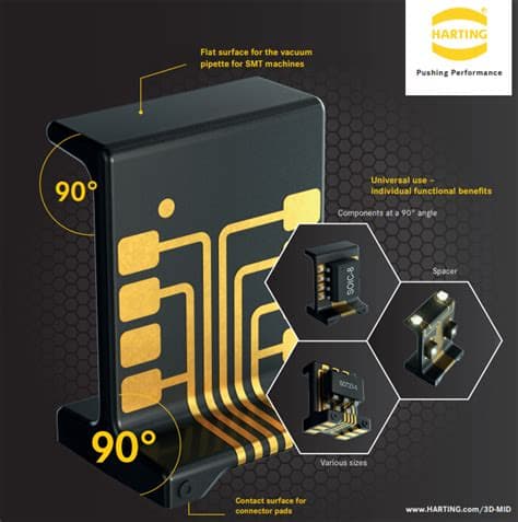
Molded Interconnect Devices, or MIDs, are three-dimensional (3D) injection-molded plastic parts with integrated electronic circuits. These devices combine the mechanical structure and electrical connectivity into a single component, eliminating the need for separate printed circuit boards (PCBs) and connectors. MIDs are made using a combination of injection molding and conductive trace patterning techniques, resulting in a highly integrated and compact solution for various electronic applications.
Applications of Molded Interconnect Devices
MIDs find applications in a wide range of industries, including:
- Automotive electronics
- Consumer electronics
- Medical devices
- Industrial automation
- Telecommunications
- Aerospace and defense
Some specific examples of MID applications include:
- Sensors and actuators
- Antennas for wireless communication devices
- Connectors and switches
- Lighting systems
- Wearable electronics
- Miniaturized medical devices

Advantages of Molded Interconnect Devices
MIDs offer several advantages over traditional PCB-based electronic assemblies:
-
Miniaturization: MIDs enable the integration of electronic circuits directly onto the surface of a 3D plastic component, resulting in significant space savings and reduced product size.
-
Weight reduction: By eliminating the need for separate PCBs and connectors, MIDs can significantly reduce the overall weight of electronic products.
-
Improved reliability: MIDs minimize the number of interconnections and solder joints, leading to improved reliability and reduced risk of failure.
-
Design flexibility: The 3D nature of MIDs allows for greater design flexibility, enabling the creation of complex shapes and geometries that are difficult or impossible to achieve with traditional PCBs.
-
Cost reduction: MIDs can reduce manufacturing costs by simplifying the assembly process, reducing the number of components, and minimizing the need for manual labor.

Manufacturing Processes for Molded Interconnect Devices
There are several manufacturing processes used to create MIDs, each with its own advantages and limitations. The most common processes include:
-
Two-Shot Molding: This process involves the injection molding of a base plastic component, followed by a second shot of a conductive plastic material to create the electrical traces.
-
Laser Direct Structuring (LDS): In this process, a laser is used to selectively activate the surface of a molded plastic part, which is then plated with a conductive material to form the electrical traces.
-
Conductive Ink Printing: This process involves the printing of conductive ink onto the surface of a molded plastic part to create the electrical traces.
-
In-Mold Electronics (IME): IME is an emerging technology that combines the injection molding process with the placement of electronic components and circuitry directly into the mold cavity.
| Manufacturing Process | Advantages | Limitations |
|---|---|---|
| Two-Shot Molding | – High design flexibility – Good mechanical properties |
– Limited to two plastic materials – Higher tooling costs |
| Laser Direct Structuring (LDS) | – High precision – Suitable for complex geometries |
– Requires specialized equipment – Limited material options |
| Conductive Ink Printing | – Low cost – Suitable for low-volume production |
– Limited conductivity – Lower durability |
| In-Mold Electronics (IME) | – High level of integration – Streamlined manufacturing process |
– Emerging technology – Limited to specific materials and components |

Future Prospects for Molded Interconnect Devices
As the demand for smaller, lighter, and more integrated electronic products continues to grow, the market for MIDs is expected to expand significantly in the coming years. According to a recent market research report, the global MID market is projected to reach USD 1.98 billion by 2025, growing at a CAGR of 11.5% from 2020 to 2025.
Several factors are driving the growth of the MID market, including:
- Increasing adoption of MIDs in the automotive industry for applications such as sensors, antennas, and lighting systems.
- Growing demand for miniaturized and wearable electronic devices in the consumer electronics and medical device sectors.
- Advancements in manufacturing technologies, such as LDS and IME, which are enabling the production of more complex and integrated MID components.
- Increasing focus on sustainability and eco-friendly manufacturing practices, which favor the use of MIDs over traditional PCB-based assemblies.
As the MID market continues to evolve, we can expect to see further innovations in materials, manufacturing processes, and applications, leading to even more advanced and integrated electronic products in the future.
Frequently Asked Questions (FAQ)
-
What are the main benefits of using Molded Interconnect Devices (MIDs) in electronic products?
MIDs offer several benefits, including miniaturization, weight reduction, improved reliability, design flexibility, and cost reduction. By integrating electronic circuits directly onto a 3D plastic component, MIDs eliminate the need for separate PCBs and connectors, resulting in more compact, lightweight, and reliable electronic products. -
What are the most common manufacturing processes used to create MIDs?
The most common manufacturing processes for MIDs include Two-Shot Molding, Laser Direct Structuring (LDS), Conductive Ink Printing, and In-Mold Electronics (IME). Each process has its own advantages and limitations, and the choice of process depends on factors such as design complexity, production volume, and material requirements. -
In which industries are MIDs most commonly used?
MIDs are used in a wide range of industries, including automotive electronics, consumer electronics, medical devices, industrial automation, telecommunications, and aerospace and defense. Some specific applications include sensors, antennas, connectors, switches, lighting systems, and wearable electronics. -
What is the future outlook for the Molded Interconnect Devices market?
The global MID market is expected to grow significantly in the coming years, driven by factors such as increasing adoption in the automotive industry, growing demand for miniaturized and wearable electronic devices, advancements in manufacturing technologies, and a focus on sustainable manufacturing practices. The market is projected to reach USD 1.98 billion by 2025, with a CAGR of 11.5% from 2020 to 2025. -
How do MIDs contribute to sustainability and eco-friendly manufacturing practices?
MIDs can contribute to sustainability and eco-friendly manufacturing practices by reducing the number of components and materials used in electronic products. By eliminating the need for separate PCBs and connectors, MIDs minimize waste and reduce the environmental impact of electronic product manufacturing. Additionally, the use of recyclable plastic materials in MIDs can further enhance their environmental benefits.
In conclusion, Molded Interconnect Devices (MIDs) represent a significant advancement in the field of electronic product design and manufacturing. By combining mechanical and electrical functionality into a single, compact component, MIDs offer numerous benefits, including miniaturization, weight reduction, improved reliability, design flexibility, and cost reduction. As the demand for more integrated and sustainable electronic products continues to grow, the market for MIDs is expected to expand significantly in the coming years, driven by advancements in manufacturing technologies and increasing adoption across various industries.
No responses yet