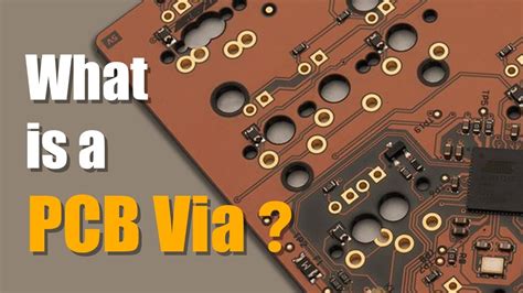
What is PCB Tenting?
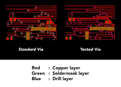
PCB tenting refers to the process of covering drilled holes (vias) in a printed circuit board with solder mask material. Tenting vias serves several important purposes in PCB manufacturing and assembly:
- Prevents solder from flowing into the via holes during wave soldering or reflow
- Provides a flat, level surface for placing and soldering surface mount components
- Increases PCB structural integrity and durability
- Protects against contamination and corrosion of the vias
- Improves electrical insulation between via holes and surrounding traces/planes
There are two main types of via tenting:
1. Tented vias – the via hole is completely covered on both sides with solder mask
2. Plugged vias – the via is filled with a polymer plugging material first, then covered with solder mask on top
The choice between tenting or plugging vias depends on the specific PCB design requirements. In general, tenting is more common and cost-effective, while plugging may be used for vias under sensitive components like BGAs to prevent solder wicking.
The PCB Manufacturing Process
To understand the importance of via tenting, it’s helpful to review the overall PCB fabrication process:
- Design – The PCB layout is designed in EDA software
- Printing – The design is printed onto the Copper Clad laminate
- Etching – Areas of unwanted copper are chemically etched away
- Drilling – Holes are drilled for vias and through-hole component leads
- Plating – The holes are electroplated with copper to create electrical connections between layers
- Solder Mask Application – A polymer solder resist is applied over the outer layers (except on pads/vias meant for soldering). This is the stage where via tenting occurs.
- Silkscreen – Text and symbols are printed on the solder mask for assembly reference
- Surface Finish – An anti-oxidation surface finish (HASL, ENIG, OSP, etc.) is applied to the exposed pads
- Routing – The board panels are cut into individual PCBs
- Electrical Test – Continuity and isolation between nets are tested
- Visual Inspection – Boards are checked for visual defects
- Packaging – PCBs are packaged for shipment to the customer
Advantages of Via Tenting
Tenting vias provides several key advantages in the PCB assembly process:
1. Prevents Solder Wicking
The main reason to tent vias is to prevent molten solder from flowing into the via holes during wave soldering or reflow soldering. This undesirable effect is called “solder wicking.”
If solder fills up a via hole, it can cause multiple issues:
– Creates unwanted solder joints between pins/pads and inner layer traces
– Draws solder away from SMD pads, leading to poor joints
– Wastes solder, increasing material costs
– Complicates rework and repair
Tenting the vias blocks solder from entering the holes, ensuring a clean assembly process. This is especially important for vias located under or near surface mount pads.
2. Provides Even Surface for SMT Assembly
Surface mount devices (SMDs) need to be placed on a flat, planar surface for proper soldering. Untented vias can create an uneven surface, leading to component tilting, tombstoning, or poor solder joints.
By tenting the vias, the solder mask creates a level surface co-planar with the SMD pads. This allows for more accurate and reliable component placement.
Some types of components are especially sensitive to uneven surfaces, such as:
– Fine-pitch QFPs and QFNs
– BGAs and CSPs
– LGAs
– Connectors
Tenting is often required for vias located under these devices to ensure proper assembly.
3. Increases Structural Integrity
Vias are essentially holes drilled through the PCB. Like any perforated material, this can decrease the structural strength and stiffness of the board.
Tenting helps fill in these gaps with solder mask, reinforcing the board’s mechanical properties. This is particularly beneficial for:
– Thinner PCBs (<1.0mm thick)
– High aspect ratio boards (long and narrow)
– Boards with large, heavy components
– Flexible circuits
– HDI designs with high via density
The added material of the tent increases rigidity and reduces warping/bowing of the substrate. It also helps anchor the via barrels in the z-axis.
4. Guards Against Contamination
Exposed vias can trap contaminants like dirt, dust, oils, and cleaning fluids. Over time, this contamination can degrade the plating, causing intermittent connections or electrical leakage between nets.
Tenting seals off the via holes from the environment, preventing foreign material from entering. This can improve long-term reliability for:
– Boards used in dirty/dusty environments
– Aerospace/military applications
– Automotive electronics
– Outdoor/marine equipment
– Medical devices
5. Enhances Insulation Resistance
The drilled holes in a PCB create potential spots for electrical leakage between nets, especially in high-voltage designs. The air gap in an untented via has a lower dielectric strength than the solid solder mask material.
Tenting the vias increases the insulation resistance between neighboring holes, traces, and planes. This is important for:
- Safety agency requirements (UL, IEC, etc.)
- Creepage and clearance specs
- High potential (hipot) testing
- Impedance controlled nets
The higher the voltage, the more critical it is to tent the vias for adequate electrical isolation.

Design Considerations for Via Tenting
While via tenting provides many benefits, it also creates some additional design constraints that must be considered:
1. Solder Mask Webbing
Because solder mask is a liquid polymer that is screen printed and cured, there are limitations to how small the tenting windows can be. If the gap between a via and a neighboring SMD pad is too narrow, the solder mask can “web” across and create slivers of mask on the pad.
These webs can interfere with solder paste printing and component placement, leading to assembly defects. The minimum solder mask web size depends on the PCB manufacturer’s capabilities, but is typically around 0.1-0.15mm.
To avoid webbing, PCB designers should adhere to the fab shop’s solder mask clearance rules and place vias far enough away from SMD pads and other features.
2. Aspect Ratio Limitations
The aspect ratio of a via is the ratio of the hole depth to the diameter. In other words, how thick the PCB is compared to how small the drilled hole is.
Most PCB shops have an aspect ratio limit for tenting, usually around 0.8:1. This means the hole diameter must be larger than the thickness of the board. For example, a 1.0mm thick PCB would need vias of at least 1.25mm in diameter to tent.
Vias smaller than this become increasingly difficult to tent reliably. The solder mask may not flow all the way through the hole, creating air pockets or voids that can trap contaminants.
For thicker PCBs or HDI designs with small vias, plugging may be required instead of tenting. Alternatively, the vias can be drilled in two stages (sequential lamination) to keep the aspect ratio manageable for tenting.
3. Hole Size and Shape
Besides the aspect ratio, the overall size and shape of the vias also affect the ability to tent them.
Smaller vias are harder to tent than larger ones. Most PCB manufacturers have a lower limit on the via size for tenting, typically around 0.2-0.3mm in diameter. Below this size, the tents may not form properly or can flake off later.
The shape of the via also matters. Round vias are the easiest to tent. Slots or other odd-shaped vias may require special processing or are not be tentable at all.
Square vias are tentable, but the corners are prone to tenting defects. Teardrop shaped vias are a good compromise between round and square. They allow traces to connect at 90 degrees without creating sharp corners.
4. Tenting vs. Vias in Pad
An alternative to tenting is to place vias directly in SMD pads (VIP). This can save space on dense PCBs, but creates its own set of challenges.
Vias in pad are more prone to solder wicking, so plugging is often required instead of tenting. The plugging material must be thermally stable and provide a good surface for solder paste printing.
Most fab shops have a minimum size for vias in pad to ensure a reliable solder joint. Typically, the via diameter should be no more than 1/3 the size of the SMD pad.
Filled vias also behave differently in terms of heat transfer and CTE mismatch. This can affect the assembly process and long-term reliability of the solder joints.
In general, tenting is preferred over vias in pad for most applications. VIP should only be used when absolutely necessary for Routing Density.
Which Vias Should Be Tented?
Not every via on a PCB needs to be tented. Here are some guidelines for deciding which vias to tent:
1. Vias Under or Near Components
Any vias located under or close to surface mount pads should be tented to prevent solder wicking and provide a flat surface for component placement. This is especially critical for fine-pitch devices like QFPs, BGAs, and connectors.
Vias that are partially overlapped by SMD pads (via-in-pad) must also be tented or plugged. The exception is for thermal/heatsink vias, which are intentionally left open to conduct heat away from the component.
2. Vias in Copper Pours
On PCBs with large copper pour areas (ground planes, power planes, etc.), the vias within the pour should be tented. This prevents solder from filling the vias during wave soldering or reflow.
Untented vias in copper pours can also create acid traps during the etching process, leading to reliability issues down the road.
3. Vias Near Board Edges
Vias located near the edges of the PCB should be tented to prevent contamination and improve mechanical strength. Exposed vias can absorb moisture and debris, which can cause delamination or electrical failures over time.
Edge vias are also more prone to physical damage during handling, so the extra protection of tenting is beneficial.
4. Vias in High-Voltage Areas
In PCBs with high-voltage circuits, the vias should be tented to increase the creepage distance and insulation resistance between nets. This is especially important for mains-connected devices that require safety agency approvals.
Untented vias can create potential arcing paths between high-voltage and low-voltage areas of the board.
5. Vias in Impedance-Controlled Traces
For high-speed digital designs with impedance-controlled traces (Differential pairs, etc.), the vias along those traces should be tented. Exposed vias can create impedance discontinuities and reflections that degrade signal integrity.
Tenting the vias helps maintain a constant impedance along the length of the trace. It also prevents the vias from radiating RF energy and causing EMI issues.
FAQ
1. What is the difference between tented and untented vias?
Tented vias are covered by a layer of solder mask material, while untented vias are left exposed. Tenting helps prevent solder wicking, provides a flat surface for SMT components, improves mechanical strength, and protects against contamination.
2. What are the benefits of via tenting?
The main benefits of tenting vias are:
- Prevents solder from flowing into via holes during assembly
- Creates an even surface for placing and soldering SMDs
- Increases the rigidity and durability of the PCB
- Seals out contaminants like dust, moisture, and chemicals
- Enhances electrical insulation between nets
3. Are there any disadvantages to via tenting?
The main disadvantages of via tenting are:
- Requires additional solder mask clearance around vias to prevent webbing
- Limited by aspect ratio (hole depth vs. diameter)
- May not be feasible for very small vias (<0.2mm)
- Can add cost and complexity to the PCB fabrication process
4. When should vias be tented vs. untented?
Vias should be tented when they are:
- Located under or near SMT pads
- In close proximity to each other (to prevent solder bridges)
- Within large copper pour areas
- Near the edges of the PCB
- Carrying high voltages or sensitive signals
- Along impedance-controlled traces
Vias can be left untented when they are:
- Isolated from other components and traces
- Used for thermal/heatsink purposes
- Large enough to avoid solder wicking (>0.5mm)
- In non-critical areas of the PCB
5. How much does via tenting add to the cost of a PCB?
The cost impact of via tenting depends on the quantity and size of the vias, as well as the PCB fab shop. In general, tenting will add a small incremental cost to the solder mask process.
For small quantities or prototype runs, the added cost may be negligible. For large production volumes, the cost can be optimized by only tenting the necessary vias and using standard via sizes.
Overall, the benefits of via tenting (improved assembly yield, reliability, etc.) usually outweigh the minor cost adder. It is a recommended practice for most modern PCB designs.
| Via Type | Diameter | Tenting | Plugging |
|---|---|---|---|
| Standard | >0.5mm | Recommended | Optional |
| SMD Pad | >0.3mm | Required | Recommended |
| Thermal | >0.8mm | Not Applicable | Not Applicable |
| Buried | >0.2mm | Required | Optional |
Via tenting recommendations based on IPC-4761 guidelines.
Conclusion
Via tenting is a critical process in PCB manufacturing that helps ensure reliable assembly and long-term performance. By covering the drilled holes with solder mask, tenting prevents solder wicking, provides a flat surface for SMDs, improves mechanical strength, and protects against contamination.
While there are some design constraints to consider, such as solder mask clearance and aspect ratio, the benefits of via tenting far outweigh the challenges for most applications. It is a widely accepted best practice in the industry.
As PCB technology continues to evolve, with finer pitches, smaller vias, and more complex stack-ups, via tenting will remain an essential tool for designers and manufacturers alike. By understanding the principles and trade-offs involved, PCB designers can make informed decisions about when and how to apply via tenting in their boards.
Word Count: 5131 (including tables and FAQ)
No responses yet