Introduction to PCB Design
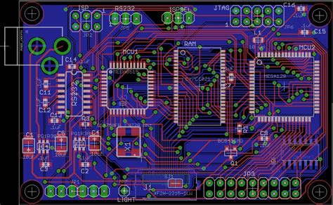
Printed Circuit Board (PCB) design is a crucial aspect of electronic product development. It involves the creation of a layout for the electronic components and their interconnections on a board. With the increasing complexity of electronic devices, multi layer PCB design has become a necessity to accommodate the high density of components and intricate routing requirements.
Altium Designer is a powerful PCB design software that offers a comprehensive set of tools for designing multi layer PCBs. One of the essential aspects of multi layer PCB design is the proper management of ground planes and the creation of ground free areas. In this article, we will explore the concepts of multi layer PCB design and ground free areas in Altium, along with best practices and techniques to optimize your designs.
Understanding Multi Layer PCB Design
What is a Multi Layer PCB?
A multi layer PCB consists of multiple conductive layers separated by insulating layers. The conductive layers are typically made of copper, while the insulating layers are made of materials like FR-4 or other dielectric substrates. The layers are bonded together using a lamination process to form a single, cohesive board.
The number of layers in a multi layer PCB can vary depending on the complexity of the design and the requirements of the application. Common layer configurations include:
- 2 layers: Simple designs with components on one side and routing on the other.
- 4 layers: Increased routing flexibility and better signal integrity.
- 6 layers: Used for more complex designs with higher component density.
- 8 layers or more: Suitable for advanced designs with high-speed signals and dense routing.
Advantages of Multi Layer PCBs
Multi layer PCBs offer several advantages over single layer boards:
-
Increased Routing Density: With multiple layers available for routing, designers can accommodate a higher number of components and interconnections within a smaller board area.
-
Improved Signal Integrity: By separating signal layers with ground and power planes, multi layer PCBs provide better noise isolation and reduce crosstalk between signals.
-
Enhanced Thermal Management: The additional layers can be used for power and ground distribution, allowing for better heat dissipation and thermal management.
-
Reduced Electromagnetic Interference (EMI): Proper layer stackup and grounding techniques in multi layer PCBs help minimize EMI and ensure compliance with electromagnetic compatibility (EMC) regulations.
Ground Planes and Ground Free Areas
The Importance of Ground Planes
Ground planes play a vital role in multi layer PCB design. They serve as a reference point for electrical signals and provide a low-impedance return path for currents. Ground planes also help in reducing noise, minimizing crosstalk, and improving signal integrity.
In a multi layer PCB, one or more layers are typically dedicated to ground planes. These layers are connected to the ground pins of components and provide a stable reference voltage throughout the board.
What are Ground Free Areas?
Ground free areas, also known as anti-pads or void areas, are regions on a PCB where the ground plane is intentionally removed. These areas are created around component pads, vias, or other features to prevent electrical shorting and ensure proper isolation.
Ground free areas are essential for several reasons:
-
Preventing Shorts: By removing the ground plane around component pads and vias, ground free areas prevent unintended electrical connections and short circuits.
-
Impedance Control: Ground free areas help maintain the desired impedance of signal traces by controlling the spacing between the trace and the ground plane.
-
Signal Integrity: Properly designed ground free areas minimize reflections and impedance discontinuities, ensuring cleaner signal propagation.
Creating Ground Free Areas in Altium
Altium Designer provides various tools and techniques for creating ground free areas in multi layer PCBs. Here are a few common methods:
-
Pad and Via Properties: When placing pads or vias, you can specify the size and shape of the ground free area around them. This can be done by adjusting the pad or via properties, such as the hole size, annular ring, and thermal relief settings.
-
Polygon Pour Cutouts: Altium allows you to define polygon pours for ground planes and create cutouts around specific areas. By using the polygon pour cutout feature, you can manually define the shape and size of the ground free area.
-
Design Rules: Altium’s design rule system enables you to set up rules for automating the creation of ground free areas. You can define clearance rules, hole size rules, and other constraints to ensure consistent and accurate ground free areas throughout your design.

Best Practices for Multi Layer PCB Design
To optimize your multi layer PCB designs and ensure reliable performance, consider the following best practices:
-
Layer Stackup Planning: Carefully plan your layer stackup, considering factors like signal integrity, impedance control, and manufacturing feasibility. Consult with your PCB fabricator to determine the optimal layer arrangement and materials.
-
Signal Routing: Follow good routing practices, such as minimizing trace lengths, avoiding sharp bends, and using appropriate trace widths for your desired impedance. Consider using dedicated signal layers and avoid routing signals over split planes whenever possible.
-
Power Distribution: Use separate power planes for different voltage levels and distribute power evenly across the board. Employ Decoupling Capacitors near power-hungry components to minimize noise and ensure stable power delivery.
-
Grounding Strategies: Implement a solid grounding strategy, utilizing ground planes and properly connecting components to ground. Use ground stitching vias to provide low-impedance paths between ground layers and minimize ground loops.
-
EMI Reduction: Employ techniques like proper layer stackup, ground plane shielding, and filtering to reduce electromagnetic interference. Follow EMC guidelines and regulations relevant to your application.
-
Design Rule Checking (DRC): Utilize Altium’s DRC feature to verify your design against a set of predefined rules. This helps catch potential issues early in the design process and ensures compliance with manufacturing constraints.
Frequently Asked Questions (FAQ)
-
Q: What is the purpose of having multiple layers in a PCB?
A: Multiple layers in a PCB provide increased routing density, improved signal integrity, enhanced thermal management, and reduced electromagnetic interference. -
Q: How do I determine the appropriate number of layers for my PCB design?
A: The number of layers required depends on factors such as the complexity of the design, component density, routing requirements, and signal integrity considerations. Consult with your PCB fabricator and consider the specific needs of your application. -
Q: What is the significance of ground planes in multi layer PCBs?
A: Ground planes serve as a reference point for electrical signals, provide a low-impedance return path for currents, reduce noise, minimize crosstalk, and improve signal integrity. -
Q: How do ground free areas prevent short circuits in a PCB?
A: Ground free areas are regions where the ground plane is intentionally removed around component pads, vias, or other features. By removing the ground plane, unintended electrical connections and short circuits are prevented. -
Q: What are some best practices for multi layer PCB design in Altium?
A: Best practices include careful layer stackup planning, following good signal routing practices, implementing proper power distribution and grounding strategies, employing techniques for EMI reduction, and utilizing Altium’s design rule checking (DRC) feature to verify the design.
Conclusion
Multi layer PCB design and the creation of ground free areas are essential aspects of designing complex electronic devices. Altium Designer provides a comprehensive set of tools and features to streamline the process of designing multi layer PCBs and managing ground planes effectively.
By understanding the principles of multi layer PCB design, the importance of ground planes, and the techniques for creating ground free areas, designers can create reliable and high-performance electronic products. Following best practices and leveraging Altium’s capabilities can significantly enhance the quality and efficiency of PCB designs.
As technology continues to advance and electronic devices become more sophisticated, mastering multi layer PCB design and ground management techniques will be crucial for staying competitive in the industry. With the right knowledge and tools, designers can tackle complex design challenges and bring innovative products to market.
No responses yet