What is PCB Grounding and Why is it Important?
PCB grounding refers to the techniques used to create a low-impedance path for electrical currents to return to their source, thus minimizing noise, electromagnetic interference (EMI), and ensuring proper functioning of the circuit. Proper grounding is essential for the stability, reliability, and performance of any electronic device.
Grounding serves several purposes:
- It provides a reference point for the circuit’s voltage levels.
- It helps to minimize noise and EMI by providing a low-impedance path for unwanted signals.
- It ensures the safety of the device and the user by preventing electrical shocks and fire hazards.
Types of Grounding in PCB Design
There are three main types of grounding techniques used in PCB design:
1. Common Ground Plane
A common ground plane is a large, continuous copper area on one or more layers of the PCB that serves as a low-impedance return path for electrical currents. This technique is the most effective in reducing EMI and ensuring proper functioning of the circuit.
Advantages of using a common ground plane:
- Provides a low-impedance return path for currents
- Minimizes EMI and crosstalk
- Improves signal integrity
- Simplifies the layout process
2. Dedicated Ground Plane
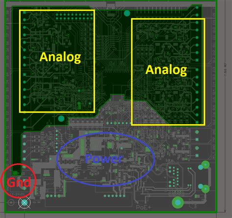
A dedicated ground plane is similar to a common ground plane but is used exclusively for a specific section of the circuit, such as analog or digital components. This technique helps to isolate sensitive parts of the circuit from noise generated by other sections.
Advantages of using a dedicated ground plane:
- Isolates sensitive circuit sections from noise
- Improves signal integrity for critical components
- Allows for better control over return currents
3. Local Ground
Local ground refers to the practice of connecting components to the ground plane through the shortest possible path. This technique helps to minimize the loop area and reduce the inductance of the return path.
Advantages of using local ground:
- Minimizes loop area and inductance
- Reduces EMI and crosstalk
- Improves signal integrity
Grounding Techniques for Different PCB Types
1. Analog and Digital Mixed-Signal PCBs
In mixed-signal PCBs, it is crucial to separate analog and digital grounds to prevent noise coupling between the two sections. Use the following techniques:
- Use a dedicated ground plane for analog components and another for digital components.
- Connect the analog and digital ground planes at a single point, preferably near the power supply.
- Use a ground plane cutout or a split plane to isolate the analog and digital sections.
2. High-Speed Digital PCBs
High-speed digital PCBs require special attention to grounding to ensure signal integrity and minimize EMI. Use these techniques:
- Use a continuous ground plane on one or more layers of the PCB.
- Minimize the loop area of return paths by placing Decoupling Capacitors close to ICs.
- Use ground vias to provide a low-impedance return path for high-frequency currents.
3. RF and Microwave PCBs
RF and microwave PCBs operate at very high frequencies and require specific grounding techniques to minimize losses and ensure proper functioning. Use these techniques:
- Use a solid, uninterrupted ground plane on the bottom layer of the PCB.
- Minimize the distance between components and the ground plane to reduce inductance.
- Use via stitching along the edges of the board to create a Faraday cage and contain EMI.

Best Practices for PCB Grounding
To ensure optimal performance and reliability of your PCB, follow these best practices:
- Use a continuous ground plane whenever possible.
- Minimize the loop area of return paths.
- Place decoupling capacitors close to ICs.
- Use ground vias to provide a low-impedance return path for high-frequency currents.
- Separate analog and digital grounds in mixed-signal PCBs.
- Use local ground connections for sensitive components.
- Avoid creating ground loops by ensuring that there is only one path to ground for each component.
- Use via stitching to contain EMI in RF and microwave PCBs.
Common Grounding Mistakes and How to Avoid Them
1. Incorrect placement of decoupling capacitors
Mistake: Placing decoupling capacitors too far from the ICs they are meant to protect.
Solution: Place decoupling capacitors as close as possible to the power pins of the ICs.
2. Improper grounding of mixed-signal PCBs
Mistake: Connecting analog and digital grounds at multiple points, creating ground loops.
Solution: Connect analog and digital grounds at a single point, preferably near the power supply.
3. Insufficient ground plane coverage
Mistake: Using a ground plane that doesn’t cover the entire PCB or has too many discontinuities.
Solution: Use a continuous ground plane whenever possible, and minimize the number of cuts or splits in the plane.
4. Incorrect use of ground vias
Mistake: Using too few or improperly placed ground vias, leading to high-impedance return paths.
Solution: Use an adequate number of ground vias, placed strategically to provide a low-impedance return path for high-frequency currents.
Grounding Techniques Comparison Table
| Technique | Advantages | Disadvantages |
|---|---|---|
| Common Ground Plane | – Low-impedance return path – Minimizes EMI and crosstalk – Improves signal integrity – Simplifies layout |
– May not be suitable for mixed-signal PCBs |
| Dedicated Ground Plane | – Isolates sensitive circuit sections – Improves signal integrity for critical components – Better control over return currents |
– Requires more PCB layers – May increase manufacturing costs |
| Local Ground | – Minimizes loop area and inductance – Reduces EMI and crosstalk – Improves signal integrity |
– May complicate the layout process – Requires careful planning |
FAQ
1. What is the difference between a ground plane and a power plane?
A ground plane is a continuous copper area on one or more layers of the PCB that serves as a low-impedance return path for electrical currents. A power plane, on the other hand, is a continuous copper area that provides a stable and low-impedance supply of power to the components on the PCB.
2. Can I use a single ground plane for both analog and digital components?
While it is possible to use a single ground plane for both analog and digital components, it is not recommended. Analog and digital components have different grounding requirements, and using a single ground plane can lead to noise coupling and signal integrity issues. It is best to use separate ground planes for analog and digital components and connect them at a single point.
3. How many ground layers should I use in my PCB?
The number of ground layers needed in a PCB depends on the complexity of the design, the frequency of operation, and the level of EMI protection required. In general, it is recommended to use at least one continuous ground plane for most PCBs. For high-speed digital or RF/microwave PCBs, multiple ground layers may be necessary to ensure proper functioning and minimize EMI.
4. What is the purpose of using decoupling capacitors in PCB grounding?
Decoupling capacitors are used to provide a low-impedance path for high-frequency currents, thus reducing noise and ensuring a stable power supply to ICs. By placing decoupling capacitors close to the power pins of ICs, you can minimize the loop area and reduce the inductance of the return path, which helps to improve signal integrity and reduce EMI.
5. How can I minimize ground loops in my PCB design?
Ground loops occur when there are multiple paths to ground for a single component, creating a loop that can act as an antenna and pick up noise. To minimize ground loops:
- Ensure that there is only one path to ground for each component.
- Use a single-point ground connection for analog and digital sections in mixed-signal PCBs.
- Avoid running ground traces in parallel with signal traces, as this can create unwanted coupling.
- Use local ground connections for sensitive components to minimize the loop area.
By following these PCB grounding techniques and best practices, you can ensure the optimal performance, reliability, and EMI protection of your electronic devices.
No responses yet