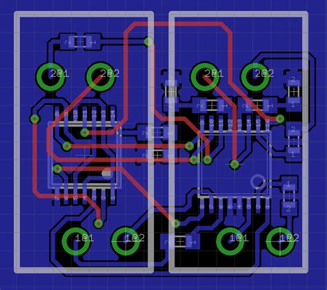
What is PCB Layout?
PCB layout, also known as printed circuit board layout, is the process of arranging and connecting all the components on a PCB to create a functional electronic device. It involves taking the schematic diagram of an electronic circuit and translating it into a physical board design that can be manufactured.
The PCB layout process is critical to the success of any electronic product. A well-designed PCB layout ensures that the device functions as intended, is reliable, and can be manufactured efficiently and cost-effectively. On the other hand, a poorly designed PCB layout can lead to a host of problems, such as signal integrity issues, electromagnetic interference (EMI), thermal management problems, and manufacturability issues.
Key Aspects of PCB Layout
There are several key aspects to consider when designing a PCB layout:
-
Component Placement: The placement of components on the PCB is crucial. Components should be arranged in a logical manner that minimizes the length of traces and reduces the risk of signal integrity issues. It’s also important to consider the mechanical constraints of the device, such as the enclosure size and shape, and the location of connectors and user interface elements.
-
Routing: Once the components are placed, the next step is to route the traces that connect them. The routing should be done in a way that minimizes crosstalk, EMI, and signal integrity issues. This may involve using techniques such as ground planes, power planes, and shielding.
-
Layers: Most PCBs have multiple layers, with each layer serving a specific purpose. For example, the top and bottom layers are typically used for component placement and routing, while the inner layers are used for power and ground planes. The number of layers needed depends on the complexity of the circuit and the required performance.
-
Vias: Vias are small holes drilled through the PCB that allow traces to connect between layers. The placement and size of vias can have a significant impact on signal integrity and manufacturability.
-
DFM: Design for Manufacturability (DFM) is an important consideration in PCB layout. The layout should be designed in a way that is easy to manufacture, with adequate clearances, tolerances, and design rules.
PCB Layout Design Service
Designing a PCB layout requires a deep understanding of electronic circuits, signal integrity, EMI, thermal management, and manufacturability. It also requires proficiency in specialized PCB design software tools such as Altium Designer, OrCAD, or Eagle.
For many companies, especially those without in-house PCB design expertise, outsourcing the PCB layout design to a specialized service provider can be a cost-effective and efficient solution. A PCB layout design service can take the schematic diagram of a circuit and create a fully manufacturable PCB layout, taking into account all the key aspects discussed above.
Benefits of Using a PCB Layout Design Service
Using a PCB layout design service offers several benefits:
-
Expertise: PCB layout design services have experienced designers who are proficient in the latest PCB design software tools and techniques. They can create high-quality layouts that are optimized for performance, reliability, and manufacturability.
-
Time and Cost Savings: Outsourcing the PCB layout design can save a significant amount of time and cost compared to doing it in-house. PCB layout design services have streamlined processes and can often complete the layout faster and more efficiently than an in-house team.
-
Scalability: PCB layout design services can scale up or down depending on the project requirements. This flexibility allows companies to handle peaks in demand without having to maintain a large in-house design team.
-
Access to Latest Tools and Technologies: PCB layout design services invest in the latest software tools and technologies to stay competitive. By outsourcing the layout design, companies can benefit from these tools and technologies without having to invest in them directly.
Choosing a PCB Layout Design Service
When choosing a PCB layout design service, there are several factors to consider:
-
Experience: Look for a service provider with extensive experience in PCB layout design, especially in your specific industry or application area.
-
Capabilities: Make sure the service provider has the capabilities to handle your specific requirements, such as the number of layers, component density, signal speeds, and manufacturing process.
-
Communication: Good communication is essential for a successful PCB layout design project. Look for a service provider that is responsive, communicative, and easy to work with.
-
Quality: Check the service provider’s quality control processes and standards. Make sure they have a robust process in place to ensure the quality and accuracy of the layout.
-
Cost: Of course, cost is always a consideration. Look for a service provider that offers competitive pricing without compromising on quality.

PCB Layout Design Process
The PCB layout design process typically involves the following steps:
-
Schematic Review: The first step is to review the schematic diagram of the circuit to ensure that it is complete, accurate, and meets all the functional requirements.
-
Component Selection: The next step is to select the specific components that will be used in the design. This involves choosing components that meet the performance, cost, and availability requirements of the project.
-
Component Placement: Once the components are selected, they are placed on the PCB layout. The placement is optimized for signal integrity, thermal management, and manufacturability.
-
Routing: After the components are placed, the traces are routed to connect them. The routing is done in a way that minimizes signal integrity issues and EMI.
-
DFM Check: The layout is then checked for Design for Manufacturability (DFM). This involves ensuring that the layout meets all the manufacturing constraints and design rules.
-
Verification: The layout is verified through simulations and design rule checks to ensure that it meets all the performance and reliability requirements.
-
Output Generation: Finally, the output files needed for manufacturing are generated. This typically includes Gerber files, drill files, and assembly drawings.

PCB Layout Design Techniques
There are several techniques that can be used to optimize the PCB layout for performance, reliability, and manufacturability. Some of these techniques include:
-
Ground Planes: Using a solid ground plane can help to reduce EMI and improve signal integrity. The ground plane provides a low-impedance return path for the signals.
-
Power Planes: Similar to ground planes, power planes can be used to distribute power efficiently across the PCB. This can help to reduce voltage drop and improve power integrity.
-
Decoupling Capacitors: Placing decoupling capacitors close to the power pins of ICs can help to reduce power supply noise and improve signal integrity.
-
Differential Pairs: For high-speed signals, using differential pairs can help to reduce EMI and improve signal integrity. Differential pairs are two traces that carry the same signal but with opposite polarity.
-
Trace Width and Spacing: The width and spacing of traces can have a significant impact on signal integrity and manufacturability. Wider traces have lower resistance and can carry more current, but they also take up more space. Spacing between traces needs to be sufficient to prevent crosstalk and short circuits.
-
Via Stitching: Using via stitching, which involves placing vias along the edges of a ground or power plane, can help to reduce EMI and improve signal integrity.
-
Thermal Management: Proper thermal management is essential for the reliability and longevity of the PCB. This can involve techniques such as using thermal vias, designing for adequate airflow, and using heat sinks or other cooling methods.

PCB Layout Design Software
There are several PCB layout design software tools available, each with its own strengths and weaknesses. Some of the most popular tools include:
| Software | Vendor | Key Features |
|---|---|---|
| Altium Designer | Altium | – Schematic capture and PCB layout – 3D modeling and visualization – Simulation and analysis tools |
| OrCAD | Cadence | – Schematic capture and PCB layout – Constraint-driven design – Integration with PSpice for simulation |
| Eagle | Autodesk | – Schematic capture and PCB layout – Large library of components – Affordable pricing for hobbyists and small businesses |
| KiCad | Open Source | – Schematic capture and PCB layout – Free and open source – Growing community and ecosystem |
The choice of software depends on factors such as the complexity of the design, the required features and capabilities, the budget, and the user’s familiarity and preference.
Frequently Asked Questions (FAQ)
- What is the difference between a schematic and a PCB layout?
-
A schematic is a symbolic representation of an electronic circuit, showing the components and their connections. A PCB layout is the physical realization of the schematic, showing the actual placement and routing of components on a printed circuit board.
-
How long does it typically take to design a PCB layout?
-
The time required to design a PCB layout varies depending on the complexity of the circuit, the number of components, and the experience of the designer. Simple designs can be completed in a few hours, while more complex designs can take several days or even weeks.
-
What are the different layers in a PCB?
- A typical PCB has several layers, including:
- Top layer: Used for component placement and routing
- Bottom layer: Also used for component placement and routing
- Inner layers: Used for power and ground planes, and additional routing
- Solder mask: A protective layer that covers the copper traces, with openings for the pads
- Silkscreen: A layer that contains text and graphics for labeling and identification
The number of layers depends on the complexity of the circuit and the required performance.
- What is DFM and why is it important?
-
DFM stands for Design for Manufacturability. It is the practice of designing the PCB layout in a way that is easy to manufacture, with adequate clearances, tolerances, and design rules. DFM is important because it helps to ensure that the PCB can be manufactured reliably and cost-effectively, with minimal defects and rework.
-
Can I use autorouting for my PCB layout?
- Autorouting is a feature in some PCB layout software tools that automatically routes the traces between components. While autorouting can be a useful tool for simple designs, it is generally not recommended for complex or high-performance designs. Autorouting may not always result in the most optimal layout, and it may not take into account all the design constraints and requirements. For best results, it is recommended to use manual routing, or to use autorouting as a starting point and then refine the layout manually.
Conclusion
PCB layout design is a critical aspect of electronic product development. A well-designed PCB layout ensures that the device functions as intended, is reliable, and can be manufactured efficiently and cost-effectively.
Outsourcing the PCB layout design to a specialized service provider can be a smart choice for companies without in-house PCB design expertise. A PCB layout design service can provide the expertise, tools, and resources needed to create high-quality layouts that are optimized for performance, reliability, and manufacturability.
When choosing a PCB layout design service, it’s important to consider factors such as experience, capabilities, communication, quality, and cost. The PCB layout design process typically involves schematic review, component selection, placement, routing, DFM check, verification, and output generation.
There are several techniques that can be used to optimize the PCB layout, such as ground planes, power planes, decoupling capacitors, differential pairs, trace width and spacing, via stitching, and thermal management. The choice of PCB layout design software depends on the specific requirements and preferences of the project.
By understanding the key aspects of PCB layout design and partnering with a reliable PCB layout design service, companies can ensure the success of their electronic products in the market.
No responses yet