Introduction
Solder balls are a common defect in surface mount technology (SMT) manufacturing that can lead to poor electrical connections, shorts, and other quality issues. Fortunately, there are several steps you can take to minimize the occurrence of solder balls and improve your SMT assembly process. In this article, we will cover 11 easy steps to help you avoid solder balls in your SMT manufacturing.
What are Solder Balls?
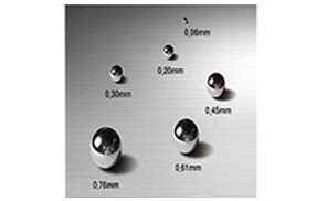
Solder balls are small spheres of solder that form on the surface of printed circuit boards (PCBs) or components during the SMT assembly process. They are typically caused by excess solder, contamination, or improper reflow profiles. Solder balls can range in size from microscopic to visible to the naked eye, and they can cause a variety of issues, including:
- Short circuits
- Open circuits
- Intermittent connections
- Reduced reliability
- Cosmetic defects

Step 1: Use High-Quality Solder Paste
The first step in Avoiding Solder Balls is to use high-quality solder paste. Solder paste is a mixture of solder powder and flux that is used to attach components to the PCB during the SMT assembly process. Using a low-quality or expired solder paste can lead to inconsistent solder joint formation and increase the risk of solder balls.
When selecting a solder paste, look for a product with the following characteristics:
- Consistent particle size distribution
- Low oxide content
- Proper viscosity and thixotropic index
- Compatible with your reflow profile and PCB surface finish

Step 2: Store Solder Paste Properly
Proper storage of solder paste is critical to maintaining its quality and preventing solder balls. Solder paste should be stored in a cool, dry place away from direct sunlight and heat sources. The ideal storage temperature for solder paste is between 0°C and 10°C (32°F and 50°F).
When storing solder paste, follow these guidelines:
- Keep the solder paste in its original container with the lid tightly sealed
- Use a refrigerator or cold storage unit specifically designed for solder paste storage
- Allow the solder paste to reach room temperature before opening the container to prevent condensation
- Use the solder paste within its shelf life, which is typically 6 months to 1 year from the date of manufacture

Step 3: Control Stencil Aperture Size and Shape
The stencil is a thin metal sheet with openings (apertures) that is used to apply solder paste to the PCB pads. The size and shape of the stencil apertures can have a significant impact on the amount of solder paste deposited and the risk of solder balls.
To minimize solder balls, follow these stencil design guidelines:
- Use a stencil thickness appropriate for your solder paste and PCB pad size (typically 0.1 to 0.15 mm)
- Design apertures with a slightly smaller area than the PCB pad to allow for solder paste spread during reflow
- Use rounded or tapered aperture corners to prevent solder paste from sticking to the stencil
- Avoid using apertures with aspect ratios (width to thickness) greater than 1.5 to prevent solder paste slumping
| Pad Size (mm) | Stencil Thickness (mm) | Aperture Size (mm) |
|---|---|---|
| 0.5 x 0.5 | 0.1 | 0.4 x 0.4 |
| 0.6 x 0.6 | 0.12 | 0.5 x 0.5 |
| 0.8 x 0.8 | 0.15 | 0.7 x 0.7 |
Step 4: Optimize Solder Paste Printing Parameters
The solder paste printing process is critical to achieving consistent solder paste deposits and preventing solder balls. To optimize your printing process, consider the following parameters:
- Print speed: Use a print speed between 20 and 60 mm/s to ensure even solder paste distribution and minimize stencil wear
- Print pressure: Apply enough pressure to ensure good contact between the stencil and PCB, but not so much that it causes solder paste to ooze out of the apertures
- Separation speed: Use a slow separation speed (1-5 mm/s) to allow the solder paste to release cleanly from the stencil and prevent solder paste tailing
- Print gap: Maintain a consistent gap between the stencil and PCB (typically 0.5 to 1 mm) to ensure even solder paste deposits and prevent solder paste bridging
Step 5: Clean the Stencil Regularly
Over time, solder paste can build up on the stencil surface and in the apertures, leading to inconsistent solder paste deposits and increasing the risk of solder balls. To prevent this, it’s important to clean the stencil regularly.
Follow these stencil cleaning guidelines:
- Clean the stencil after every print cycle or every 10-20 PCBs, depending on the solder paste volume and print quality
- Use a lint-free wipe and a compatible cleaning solvent (isopropyl alcohol or a commercial stencil cleaner) to remove solder paste residue
- Inspect the stencil for any damage or clogged apertures and replace or repair as needed
- Store the stencil in a protective cover when not in use to prevent contamination and damage
Step 6: Control PCB and Component Cleanliness
Contamination on the PCB or component surfaces can interfere with solder paste adhesion and cause solder balls. To minimize contamination, follow these guidelines:
- Handle PCBs and components with gloves to prevent oils and dirt from transferring to the surfaces
- Store PCBs and components in a clean, dry environment away from dust and moisture
- Clean PCBs and components with isopropyl alcohol or a compatible cleaning agent before assembly
- Bake moisture-sensitive components before assembly to remove any absorbed moisture that could cause solder spattering during reflow
Step 7: Optimize Reflow Profile
The reflow profile is the temperature and time profile used to melt the solder paste and form solder joints during the SMT assembly process. An improper reflow profile can lead to solder ball formation, as well as other defects like solder bridging and tombstoning.
To optimize your reflow profile, consider the following factors:
- Preheat rate: Use a gradual preheat rate (1-3°C/s) to allow the PCB and components to reach a stable temperature and activate the flux in the solder paste
- Soak time: Allow sufficient soak time (60-120 seconds) for the flux to remove oxides and prepare the surfaces for solder wetting
- Peak temperature: Ensure the peak temperature reaches the solder paste manufacturer’s recommended value (typically 20-40°C above the solder melting point) to achieve complete solder melting and wetting
- Cooling rate: Use a controlled cooling rate (1-4°C/s) to allow the solder joints to solidify without excessive stress or intermetallic growth
Here’s an example reflow profile for a lead-free solder paste:
| Zone | Temperature (°C) | Time (seconds) |
|---|---|---|
| Preheat | 25 to 150 | 60 to 90 |
| Soak | 150 to 180 | 60 to 120 |
| Reflow | 180 to 245 | 30 to 60 |
| Peak | 245 to 260 | 10 to 30 |
| Cooling | 260 to 100 | 60 to 120 |
Step 8: Use Nitrogen in Reflow Oven
Using nitrogen in the reflow oven can help reduce solder ball formation by limiting the amount of oxygen available to form oxides on the solder surface. Nitrogen also helps improve solder joint strength and appearance by creating a more inert atmosphere.
When using nitrogen in your reflow oven, consider the following:
- Use a nitrogen purity of at least 99.999% to minimize contaminants
- Maintain a nitrogen flow rate sufficient to displace the air in the oven (typically 10-20 cubic feet per minute)
- Monitor the oxygen level in the oven and aim for a concentration below 100 ppm during the reflow process
- Ensure proper ventilation and safety precautions when using nitrogen, as it can displace breathable air
Step 9: Implement SPI and AOI Inspection
Solder paste inspection (SPI) and automated optical inspection (AOI) are two techniques that can help identify solder ball issues early in the SMT assembly process.
- SPI: SPI systems use 3D imaging to measure the volume, height, and position of solder paste deposits after printing. This allows you to detect any inconsistencies or defects in the solder paste before component placement and reflow.
- AOI: AOI systems use high-resolution cameras and image analysis software to inspect the assembled PCB for solder balls, bridging, tombstoning, and other defects after reflow. This allows you to catch any issues before the PCB moves on to further testing or assembly.
By implementing SPI and AOI in your SMT assembly process, you can quickly identify and correct any solder ball issues, reducing rework and improving overall quality.
Step 10: Conduct Regular Maintenance and Calibration
Regular maintenance and calibration of your SMT equipment can help prevent solder ball issues by ensuring consistent and accurate performance. Follow these maintenance and calibration guidelines:
- Perform daily, weekly, and monthly cleaning and inspection of your stencil printer, pick-and-place machine, and reflow oven
- Check and adjust the alignment and calibration of your equipment according to the manufacturer’s recommendations
- Replace any worn or damaged parts, such as stencil wipers, pick-and-place nozzles, or conveyor belts
- Monitor and record key process parameters, such as print pressure, placement force, and reflow temperatures, to identify any trends or anomalies
Step 11: Train and Educate Operators
Finally, proper training and education of your SMT operators can go a long way in preventing solder ball issues. Ensure your operators are trained on the following:
- Proper handling and storage of solder paste and other materials
- Correct setup and operation of SMT equipment
- Visual inspection of solder paste prints and assembled PCBs
- Identification and troubleshooting of common SMT defects, including solder balls
- Safety procedures and personal protective equipment (PPE) usage
By investing in operator training and education, you can create a more skilled and knowledgeable workforce that is better equipped to prevent and solve solder ball issues.
Frequently Asked Questions
What causes solder balls in SMT assembly?
Solder balls can be caused by various factors, including:
– Excess solder paste
– Contamination on the PCB or component surfaces
– Improper reflow profile
– Stencil aperture size and shape issues
– Inadequate cleaning of the stencil or PCB
How can I detect solder balls on my assembled PCBs?
Solder balls can be detected using various inspection methods, such as:
– Visual inspection with a magnifying lens or microscope
– Automated optical inspection (AOI) systems
– X-ray inspection for hidden solder balls under components
Can solder balls cause reliability issues in my PCBs?
Yes, solder balls can cause reliability issues by creating short circuits, intermittent connections, or other defects that can lead to PCB failure over time. It’s important to minimize solder balls to ensure the long-term reliability of your PCBs.
How often should I clean my stencil to prevent solder balls?
The frequency of stencil cleaning depends on factors like solder paste volume, print quality, and production rate. As a general guideline, clean the stencil after every print cycle or every 10-20 PCBs to prevent solder paste buildup and solder ball formation.
What is the ideal reflow profile for preventing solder balls?
The ideal reflow profile depends on the specific solder paste and PCB design, but in general, it should include:
– Gradual preheat to activate the flux and stabilize the PCB and components
– Sufficient soak time to remove oxides and prepare the surfaces for solder wetting
– Peak temperature above the solder melting point to ensure complete solder melting and wetting
– Controlled cooling to allow the solder joints to solidify without excessive stress or intermetallic growth
Consult your solder paste manufacturer’s recommendations and perform profile tuning to optimize your reflow profile for your specific application.
Conclusion
Solder balls are a common defect in SMT assembly that can lead to quality and reliability issues in your PCBs. By following the 11 easy steps outlined in this article, you can significantly reduce the occurrence of solder balls and improve your SMT manufacturing process.
Remember to use high-quality materials, maintain proper storage and handling procedures, optimize your stencil design and printing parameters, implement regular cleaning and inspection, and invest in operator training and education. By taking a holistic approach to solder ball prevention, you can achieve more consistent and reliable SMT assembly results.
No responses yet