Introduction to PCB Soldering Issues
Printed Circuit Board (PCB) soldering is a crucial process in the manufacturing of electronic devices. It involves attaching electronic components to the PCB using solder, a metal alloy that melts at a relatively low temperature. Proper PCB soldering ensures that the electronic device functions correctly and reliably. However, several issues can arise during the PCB soldering process that can affect the quality and reliability of the final product. In this article, we will discuss 10 critical issues that we need to pay attention to in PCB soldering.
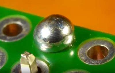
Issue 1: Poor Solder Joint Formation
Poor solder joint formation is one of the most common issues in PCB soldering. It occurs when the solder does not properly wet the surfaces of the component leads and PCB pads, resulting in a weak or incomplete connection. Several factors can contribute to poor solder joint formation, including:
- Insufficient solder: If there is not enough solder applied to the joint, it may not form a strong connection.
- Incorrect solder temperature: If the solder is too cold, it may not flow properly and form a good connection. If the solder is too hot, it may damage the components or cause the solder to wick away from the joint.
- Contaminated surfaces: If the component leads or PCB pads are contaminated with dirt, oil, or oxidation, the solder may not adhere properly.
To prevent poor solder joint formation, it is essential to use the correct amount of solder, maintain the proper solder temperature, and ensure that all surfaces are clean and free of contamination.

Issue 2: Bridging
Bridging occurs when solder inadvertently connects two or more adjacent pins or pads on the PCB. This can happen when too much solder is applied or when the solder is not properly controlled during the soldering process. Bridging can cause short circuits and other functional issues in the electronic device.
To prevent bridging, it is important to use the appropriate amount of solder and to carefully control the soldering process. Using a microscope or magnifying glass to inspect the solder joints can also help identify and correct any bridging issues.

Issue 3: Cold Solder Joints
Cold solder joints occur when the solder does not melt completely, resulting in a dull, grainy appearance and a weak connection. This can happen when the soldering iron is not hot enough, when the solder is applied too quickly, or when there is insufficient flux.
To prevent cold solder joints, it is essential to use a soldering iron with the appropriate temperature for the solder being used and to apply the solder slowly and evenly. Using enough flux can also help the solder flow more easily and form a stronger connection.

Issue 4: Tombstoning
Tombstoning, also known as “Manhattan effect” or “drawbridging”, occurs when a surface-mount component stands up on one end during the soldering process. This can happen when there is an imbalance in the solder volume or heat on either side of the component, causing one end to lift off the PCB.
To prevent tombstoning, it is important to ensure that the solder paste is applied evenly on both pads and that the component placement is accurate. Using a slower ramp-up rate during the reflow process can also help prevent tombstoning.
Issue 5: Solder Balling
Solder balling occurs when small balls of solder adhere to the component leads or PCB pads during the soldering process. This can happen when there is too much solder or when the solder is overheated, causing it to splatter.
To prevent solder balling, it is important to use the appropriate amount of solder and to carefully control the soldering temperature. Using a nitrogen atmosphere during the reflow process can also help reduce oxidation and prevent solder balling.
Issue 6: Insufficient Wetting
Insufficient wetting occurs when the solder does not flow evenly over the surfaces of the component leads and PCB pads. This can result in a weak or incomplete connection and can cause reliability issues over time.
To prevent insufficient wetting, it is essential to ensure that all surfaces are clean and free of contamination, and that the solder is applied evenly and at the appropriate temperature. Using enough flux can also help the solder flow more easily and form a stronger connection.
Issue 7: Lifted Pads
Lifted pads occur when the copper pad on the PCB separates from the board during the soldering process. This can happen when there is too much stress on the pad, such as when a component is misaligned or when the PCB is handled roughly.
To prevent lifted pads, it is important to ensure that components are properly aligned and that the PCB is handled gently during the soldering process. Using a support pin or adhesive to hold the component in place can also help reduce stress on the pads.
Issue 8: Flux Residue
Flux is a chemical used in the soldering process to help the solder flow more easily and form a stronger connection. However, if the flux is not properly cleaned off after soldering, it can leave a residue on the PCB that can cause corrosion or other issues over time.
To prevent flux residue, it is essential to use a compatible cleaning solution and to thoroughly clean the PCB after the soldering process. Using a no-clean flux can also help reduce the amount of residue left on the board.
Issue 9: Thermal Damage
Thermal damage can occur when the soldering iron or reflow oven is too hot, causing damage to the components or PCB. This can result in reduced reliability or complete failure of the electronic device.
To prevent thermal damage, it is important to use the appropriate temperature for the solder and components being used, and to carefully control the soldering process. Using a temperature-controlled soldering iron or reflow oven can also help ensure that the temperature remains within the appropriate range.
Issue 10: Electrostatic Discharge (ESD) Damage
Electrostatic discharge (ESD) can occur when static electricity builds up on the PCB or components and is suddenly discharged, causing damage to sensitive electronic components.
To prevent ESD damage, it is important to use proper ESD protection measures, such as grounding straps, ESD-safe mats, and ionizers. Handling PCBs and components carefully and avoiding contact with conductive surfaces can also help reduce the risk of ESD damage.
| Issue | Causes | Prevention |
|---|---|---|
| Poor Solder Joint Formation | Insufficient solder, incorrect temperature, contaminated surfaces | Use correct amount of solder, maintain proper temperature, clean surfaces |
| Bridging | Too much solder, uncontrolled soldering process | Use appropriate amount of solder, control soldering process, inspect with magnification |
| Cold Solder Joints | Low soldering iron temperature, quick solder application, insufficient flux | Use appropriate soldering iron temperature, apply solder slowly and evenly, use enough flux |
| Tombstoning | Imbalance in solder volume or heat, inaccurate component placement | Apply solder paste evenly, ensure accurate component placement, use slower ramp-up rate |
| Solder Balling | Too much solder, overheated solder | Use appropriate amount of solder, control soldering temperature, use nitrogen atmosphere |
| Insufficient Wetting | Contaminated surfaces, uneven solder application, incorrect temperature | Clean surfaces, apply solder evenly at appropriate temperature, use enough flux |
| Lifted Pads | Stress on pads from misaligned components or rough handling | Ensure proper component alignment, handle PCB gently, use support pin or adhesive |
| Flux Residue | Improper cleaning, incompatible cleaning solution | Thoroughly clean PCB, use compatible cleaning solution, use no-clean flux |
| Thermal Damage | Excessive soldering iron or reflow oven temperature | Use appropriate temperature for solder and components, control soldering process, use temperature-controlled equipment |
| ESD Damage | Static electricity buildup and sudden discharge | Use ESD protection measures, handle PCBs and components carefully, avoid contact with conductive surfaces |
Frequently Asked Questions (FAQ)
1. What is the most common issue in PCB soldering?
The most common issue in PCB soldering is poor solder joint formation, which can result from insufficient solder, incorrect solder temperature, or contaminated surfaces.
2. How can I prevent bridging during PCB soldering?
To prevent bridging, use the appropriate amount of solder and carefully control the soldering process. Inspecting the solder joints with a microscope or magnifying glass can also help identify and correct any bridging issues.
3. What causes cold solder joints?
Cold solder joints can occur when the soldering iron is not hot enough, when the solder is applied too quickly, or when there is insufficient flux.
4. How can I prevent tombstoning during the reflow process?
To prevent tombstoning, ensure that the solder paste is applied evenly on both pads and that the component placement is accurate. Using a slower ramp-up rate during the reflow process can also help.
5. What is the best way to prevent ESD damage during PCB soldering?
To prevent ESD damage, use proper ESD protection measures, such as grounding straps, ESD-safe mats, and ionizers. Handling PCBs and components carefully and avoiding contact with conductive surfaces can also help reduce the risk of ESD damage.
Conclusion
PCB soldering is a critical process in the manufacturing of electronic devices, and it is essential to pay attention to the various issues that can arise during this process. By understanding the causes and prevention methods for each issue, manufacturers can ensure that their PCBs are of high quality and reliability. Using the appropriate tools, materials, and techniques, and following best practices for PCB soldering, can help minimize the occurrence of these issues and improve the overall performance of the electronic device.
No responses yet