What is SMT PCB Assembly?
Surface-mount technology (SMT) PCB assembly is a method for producing electronic circuits in which the components are mounted directly onto the surface of printed circuit boards (PCBs). This technology has largely replaced the through-hole technology construction method of fitting components with wire leads into holes in the circuit board.
SMT PCB assembly offers several advantages over through-hole manufacturing, including:
- Smaller components and higher circuit densities
- Faster and more efficient assembly processes
- Lower production costs
- Improved mechanical performance under shake and vibration conditions
The SMT PCB assembly process involves several key steps, which we will cover in detail in the following sections.
Step 1: Design and Preparation
PCB Design
The first step in the SMT PCB assembly process is designing the printed circuit board. This involves creating a schematic diagram and a PCB layout using specialized software such as Altium Designer, Eagle, or KiCad.
When designing the PCB, consider the following factors:
- Component placement and orientation
- Trace width and spacing
- Via size and placement
- Power and ground plane design
- Signal integrity and electromagnetic compatibility (EMC)
Bill of Materials (BOM) Creation
Once the PCB design is complete, create a bill of materials (BOM) that lists all the components required for the assembly. The BOM should include the following information for each component:
- Reference designator
- Manufacturer part number
- Description
- Quantity
- Package type and size
Gerber File Generation
After finalizing the PCB design, generate Gerber files, which are standard file formats used to describe the printed circuit board images. These files include information on the copper layers, solder mask, silkscreen, and drill holes.

Step 2: Solder Paste Stencil Printing
Solder Paste
Solder paste is a mixture of tiny solder particles suspended in a flux medium. The solder paste is applied to the PCB pads where components will be placed. The most common solder paste types are lead-based (SnPb) and lead-free (SAC305).
Stencil Printing
A stencil is a thin metal sheet with apertures that correspond to the PCB pads. The stencil is aligned with the PCB, and solder paste is spread over the stencil using a squeegee. The solder paste is deposited onto the PCB pads through the stencil apertures.
Factors affecting stencil printing quality include:
- Stencil thickness and material
- Aperture size and shape
- Solder paste properties (viscosity, particle size, etc.)
- Squeegee pressure and speed
- PCB and stencil alignment

Step 3: Component Placement
Pick and Place Machine
A pick and place (P&P) machine is used to automatically place SMT components onto the PCB. The machine uses a vacuum nozzle to pick up components from feeders and place them on the solder paste-coated pads.
Modern P&P machines offer the following features:
- High-speed placement (up to 100,000 components per hour)
- High-precision placement (±0.025 mm)
- Vision systems for component alignment and inspection
- Multi-nozzle heads for simultaneous placement
- Feeders for various component package types (reels, trays, sticks)
Component Placement Sequence
The P&P machine follows an optimized placement sequence to minimize the distance traveled by the nozzle head and maximize the assembly speed. The placement sequence is generated by the machine’s software based on the PCB layout and component information.

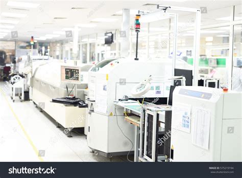
Step 4: Reflow Soldering
Reflow Oven
After component placement, the PCB is conveyed through a reflow oven, which applies a controlled temperature profile to melt the solder paste and form permanent electrical and mechanical connections between the components and PCB pads.
A typical reflow temperature profile consists of four stages:
- Preheat: The PCB is gradually heated to activate the flux and evaporate the solvent.
- Thermal soak: The temperature is maintained to allow the components and PCB to reach a uniform temperature.
- Reflow: The temperature is raised above the solder’s melting point, causing the solder to melt and form interconnections.
- Cooling: The PCB is cooled to solidify the solder joints.
Reflow Soldering Process Optimization
To ensure high-quality solder joints, optimize the reflow soldering process by considering the following factors:
- Reflow temperature profile (ramp rates, peak temperature, time above liquidus)
- Solder paste and component compatibility
- PCB and component thermal mass
- Oven conveyor speed and airflow
Step 5: Inspection and Quality Control
Visual Inspection
After reflow soldering, visually inspect the PCB for defects such as:
- Solder bridges
- Cold solder joints
- Tombstoning (component standing on one end)
- Insufficient or excessive solder
- Component misalignment or missing components
Automated Optical Inspection (AOI)
AOI systems use cameras and image processing algorithms to automatically detect assembly defects. AOI systems can identify defects that are difficult to spot with the naked eye and provide fast, objective, and repeatable inspection results.
X-Ray Inspection
X-ray inspection is used to detect defects in hidden solder joints, such as those under ball grid array (BGA) packages. X-ray systems can reveal voids, cracks, and insufficient solder in these hard-to-inspect areas.
Step 6: Rework and Repair
If defects are found during the inspection process, rework and repair the PCB as necessary. This may involve:
- Removing and replacing defective components
- Adding or removing solder using a soldering iron or hot air rework station
- Cleaning and re-applying solder paste to the affected areas
Document all rework and repair activities for traceability and process improvement purposes.
Step 7: Conformal Coating (Optional)
Conformal coating is a protective layer applied to the PCB to shield it from environmental factors such as moisture, dust, and chemicals. Common conformal coating materials include:
- Acrylic
- Silicone
- Polyurethane
- Epoxy
Apply the conformal coating using methods such as spraying, dipping, or brushing, depending on the PCB geometry and coating material properties.
Step 8: Final Assembly and Packaging
Final Assembly
After the SMT PCB assembly process is complete, perform any necessary final assembly steps, such as:
- Attaching through-hole components
- Connecting wires, cables, or connectors
- Installing the PCB into the enclosure or housing
Packaging and Shipping
Package the assembled PCBs in anti-static bags and protective boxes to prevent damage during shipping. Label the packages with relevant information, such as:
- Part number and revision
- Quantity
- Date of manufacture
- Lot or batch number
Ship the packaged PCBs to the customer or the next stage in the production process.
Step 9: Documentation and Continuous Improvement
Documentation
Maintain accurate and up-to-date documentation for the SMT PCB assembly process, including:
- PCB design files (schematics, layouts, Gerber files)
- Bill of materials (BOM)
- Assembly work instructions
- Quality control and inspection procedures
- Rework and repair logs
Continuous Improvement
Continuously monitor and improve the SMT PCB assembly process by:
- Collecting and analyzing process data (defect rates, cycle times, yields)
- Identifying root causes of problems and implementing corrective actions
- Updating processes and documentation based on lessons learned
- Investing in new technologies and equipment to enhance efficiency and quality
By following these nine detailed steps and continuously improving your processes, you can ensure the successful completion of your SMT PCB assembly projects.
Frequently Asked Questions (FAQ)
Q1: What is the difference between SMT and through-hole PCB assembly?
A1: SMT (surface-mount technology) PCB assembly involves mounting components directly onto the surface of the PCB, while through-hole assembly requires inserting component leads through holes in the PCB and soldering them on the opposite side. SMT allows for smaller components, higher circuit densities, and faster assembly compared to through-hole technology.
Q2: What factors should I consider when selecting a solder paste for SMT PCB assembly?
A2: When choosing a solder paste, consider factors such as the alloy composition (lead-based or lead-free), particle size and shape, flux type and activity, viscosity, and compatibility with the PCB surface finish and components. Consult with your solder paste supplier and conduct trials to determine the best solder paste for your specific application.
Q3: How can I optimize the reflow soldering process for my SMT PCB assembly?
A3: To optimize the reflow soldering process, develop a suitable temperature profile that considers the solder paste and component requirements, PCB thermal mass, and oven capabilities. Monitor the process using thermocouples and adjust the profile as needed to achieve consistent, high-quality solder joints. Regular maintenance and calibration of the reflow oven are also essential for process stability.
Q4: What are some common defects encountered in SMT PCB assembly, and how can they be prevented?
A4: Common SMT PCB assembly defects include solder bridges, cold solder joints, tombstoning, insufficient or excessive solder, and component misalignment. To prevent these defects, ensure proper stencil design and printing, optimize the reflow soldering process, use appropriate component placement techniques, and implement robust inspection and quality control procedures.
Q5: How can I choose the right conformal coating for my SMT PCB assembly?
A5: When selecting a conformal coating, consider the environmental protection requirements, PCB geometry, component compatibility, and application method. Evaluate the coating material properties, such as dielectric strength, moisture resistance, thermal stability, and ease of application and removal. Conduct compatibility tests and trial runs to validate the coating performance before implementing it in production.
No responses yet