What is PCB Delamination?
PCB delamination is a defect characterized by the separation of layers within a printed circuit board. It occurs when the adhesive bond between the copper foil and the substrate, or between the substrate layers themselves, fails. This failure results in the formation of blisters or bubbles on the surface of the PCB, which can lead to various problems, including electrical shorts, open circuits, and reduced board strength.
Types of PCB Delamination
There are two main types of PCB delamination:
-
Copper-to-substrate delamination: This type of delamination occurs when the copper foil separates from the substrate material, such as FR-4 or polyimide. It is often caused by poor adhesion between the copper and the substrate during the manufacturing process.
-
Substrate-to-substrate delamination: This type of delamination involves the separation of the substrate layers themselves. It can occur between the core layers or between the prepreg layers in a multi-layer PCB.
Causes of PCB Delamination
Several factors can contribute to the occurrence of PCB delamination:
Moisture Absorption
One of the primary causes of PCB delamination is moisture absorption. When a PCB is exposed to humid environments, the substrate material can absorb moisture, causing it to expand. During the soldering process, the rapid heating of the board can cause the moisture to vaporize, creating steam pressure that pushes the layers apart, resulting in delamination.
Thermal Stress
Thermal stress is another significant contributor to PCB delamination. During the assembly process, PCBs undergo multiple heating and cooling cycles, such as during soldering or reflow. If the coefficient of thermal expansion (CTE) of the copper and substrate materials is not well-matched, the resulting stress can cause the layers to separate, leading to delamination.
Manufacturing Defects
PCB delamination can also be caused by various manufacturing defects, such as:
- Poor lamination process control
- Inadequate pressure or temperature during lamination
- Contamination of the substrate or copper surfaces
- Improper handling or storage of materials
Material Selection
The choice of materials used in PCB fabrication can also influence the likelihood of delamination. Using low-quality or incompatible materials, such as substrates with poor adhesion properties or copper foils with incorrect surface treatments, can increase the risk of delamination.

Effects of PCB Delamination
PCB delamination can have severe consequences on the performance and reliability of electronic devices:
Electrical Failures
Delamination can cause electrical failures in several ways:
- Short circuits: When the copper foil separates from the substrate, it can come into contact with adjacent conductors, causing short circuits.
- Open circuits: Delamination can also lead to open circuits if the copper traces crack or break due to the separation of layers.
- Intermittent connections: In some cases, delamination may cause intermittent connections, where the circuit functions properly under certain conditions but fails under others, such as changes in temperature or vibration.
Mechanical Weakening
Delamination can significantly reduce the mechanical strength of a PCB. As the layers separate, the board becomes more susceptible to bending, warping, and cracking under stress. This weakening can lead to premature failure of the PCB and the electronic device it supports.
Thermal Management Issues
Delamination can also compromise the thermal management of a PCB. When the layers separate, air gaps form between them, reducing the board’s ability to dissipate heat effectively. This can lead to localized hot spots and accelerated aging of the PCB and its components.
Reliability Concerns
The presence of delamination in a PCB raises serious concerns about the overall reliability of the electronic device. Delaminated boards are more likely to fail prematurely, leading to increased warranty claims, customer dissatisfaction, and damage to the manufacturer’s reputation.

Prevention of PCB Delamination
To minimize the risk of PCB delamination, several prevention strategies can be employed:
Moisture Management
Proper moisture management is crucial to preventing delamination. This can be achieved through:
- Baking: Prior to assembly, PCBs should be baked to remove any absorbed moisture. The baking time and temperature depend on the board thickness and the level of moisture sensitivity.
- Moisture barrier bags: Storing PCBs in moisture barrier bags with desiccants can help prevent moisture absorption during transportation and storage.
- Controlled environment: Maintaining a controlled environment with low humidity during PCB manufacturing and assembly can reduce the risk of moisture-related delamination.
Thermal Management
Minimizing thermal stress is essential to preventing delamination. This can be accomplished by:
- Material selection: Choosing substrate and copper materials with closely matched CTEs can help reduce thermal stress during temperature cycling.
- Gradual heating and cooling: Implementing gradual heating and cooling cycles during assembly processes, such as soldering or reflow, can minimize thermal shock and reduce the risk of delamination.
Quality Control
Strict quality control measures should be implemented throughout the PCB manufacturing process to prevent defects that can lead to delamination:
- Incoming material inspection: All incoming materials should be inspected for quality and conformance to specifications.
- Process control: Lamination parameters, such as pressure, temperature, and time, should be carefully monitored and controlled to ensure consistent adhesion between layers.
- Cleanliness: Maintaining a clean manufacturing environment and ensuring the cleanliness of the substrate and copper surfaces can prevent contamination that may weaken the adhesive bond.
Design Considerations
PCB designers can also take steps to minimize the risk of delamination:
- Balanced copper distribution: Ensuring a balanced copper distribution across the layers can help reduce thermal stress and minimize the risk of delamination.
- Proper via design: Designing vias with appropriate sizes and spacing can help prevent localized stress concentrations that may lead to delamination.
- Strain relief: Incorporating strain relief features, such as flexible interconnects or underfill materials, can help absorb thermal and mechanical stresses, reducing the likelihood of delamination.

Detecting PCB Delamination
Detecting PCB delamination is crucial for ensuring the quality and reliability of electronic devices. Several methods can be used to identify delamination:
Visual Inspection
Visual inspection is the most basic method for detecting delamination. Operators can visually examine the PCB surface for signs of blistering, bubbling, or separation of layers. However, this method is limited to detecting delamination that is visible on the surface and may not identify internal delamination.
Acoustic Microscopy
Acoustic microscopy is a non-destructive testing method that uses high-frequency sound waves to create images of the internal structure of a PCB. This technique can detect delamination, voids, and other internal defects that may not be visible on the surface.
X-ray Inspection
X-ray inspection is another non-destructive testing method that can reveal internal delamination in PCBs. X-rays pass through the board, creating images that show the density variations caused by delamination or other defects.
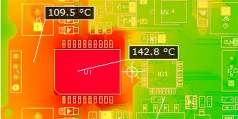
Thermal Imaging
Thermal imaging can be used to detect delamination by identifying areas of the PCB that exhibit abnormal thermal behavior. Delaminated regions may appear as hot spots or areas with reduced thermal conductivity, indicating the presence of air gaps between layers.
Destructive Testing
In some cases, destructive testing may be necessary to confirm the presence and extent of delamination. Cross-sectioning and microsectioning techniques involve cutting the PCB and examining the cut surface under a microscope to assess the adhesion between layers.
Repairing PCB Delamination
Repairing PCB delamination is often challenging and may not be feasible in all cases. The success of the repair depends on the extent and location of the delamination, as well as the availability of suitable repair materials and techniques.
Epoxy Injection
For minor, localized delamination, epoxy injection may be a viable repair option. This involves injecting a specialized epoxy resin into the delaminated area to fill the gaps and restore the adhesive bond between layers. However, this method may not be suitable for extensive delamination or cases where the delamination affects critical circuit features.
Rework and Replacement
In many cases, the best course of action for dealing with PCB delamination is to rework or replace the affected board. Rework involves removing the delaminated portion of the PCB and replacing it with a new section, either by splicing or using a replacement module. If the delamination is extensive or affects critical components, complete replacement of the PCB may be necessary to ensure the reliability and functionality of the electronic device.
FAQ
-
What is the main cause of PCB delamination?
The main cause of PCB delamination is moisture absorption, which can lead to the expansion of the substrate material and the formation of steam pressure during the soldering process, causing the layers to separate. -
Can PCB delamination be detected visually?
Yes, PCB delamination can often be detected visually by examining the surface of the board for signs of blistering, bubbling, or separation of layers. However, visual inspection may not reveal internal delamination. -
Is it possible to repair PCB delamination?
Repairing PCB delamination is possible in some cases, particularly for minor, localized delamination. Epoxy injection can be used to fill the gaps and restore the adhesive bond between layers. However, extensive delamination may require rework or complete replacement of the PCB. -
How can PCB delamination be prevented?
PCB delamination can be prevented through proper moisture management (baking, moisture barrier bags, controlled environment), thermal management (material selection, gradual heating and cooling), strict quality control measures, and appropriate design considerations (balanced copper distribution, proper via design, strain relief). -
What are the consequences of PCB delamination?
The consequences of PCB delamination include electrical failures (short circuits, open circuits, intermittent connections), mechanical weakening, thermal management issues, and reduced reliability of the electronic device. Delamination can lead to premature failure, increased warranty claims, and damage to the manufacturer’s reputation.
In conclusion, PCB delamination is a critical defect that can have severe consequences for the performance and reliability of electronic devices. By understanding the causes, effects, and prevention methods of delamination, manufacturers can take proactive steps to minimize its occurrence and ensure the production of high-quality, reliable PCBs. Through a combination of proper material selection, process control, design considerations, and quality assurance measures, the risk of PCB delamination can be significantly reduced, leading to improved product quality and customer satisfaction.
| Cause | Prevention Method |
|---|---|
| Moisture Absorption | Baking, moisture barrier bags, controlled environment |
| Thermal Stress | Material selection, gradual heating and cooling |
| Manufacturing Defects | Strict quality control measures |
| Material Selection | Choosing compatible, high-quality materials |
Table 1: Causes of PCB delamination and their corresponding prevention methods.
| Detection Method | Description |
|---|---|
| Visual Inspection | Examining the PCB surface for signs of delamination |
| Acoustic Microscopy | Using high-frequency sound waves to create internal images |
| X-ray Inspection | Using X-rays to reveal internal delamination |
| Thermal Imaging | Identifying abnormal thermal behavior in delaminated areas |
| Destructive Testing | Cross-sectioning or microsectioning to assess adhesion |
Table 2: Methods for detecting PCB delamination.
No responses yet