What are Castellated Holes?
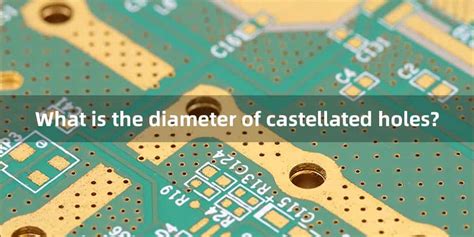
Castellated holes, also known as castellations or half-vias, are a type of mounting hole used in printed circuit board (PCB) design and production. Unlike traditional plated through-holes that are completely surrounded by copper, castellated holes are located along the edge of a PCB and are only plated on one side, resembling the battlements of a castle wall.
Castellated holes offer several advantages in PCB production, including:
- Allowing for easy board-to-board connections
- Providing mechanical support for mounted components
- Enabling efficient panelization and depanelization of PCBs
- Facilitating high-density designs with limited space
In this article, we will explore the use of castellated holes in PCB production, covering design considerations, manufacturing processes, and best practices for incorporating them into your projects.
Design Considerations for Castellated Holes
When designing a PCB with castellated holes, there are several factors to consider to ensure optimal performance and manufacturability:
1. Hole Size and Spacing
The size and spacing of castellated holes depend on the specific requirements of your project, such as the components being used and the desired board-to-board connection method. Typical castellated hole sizes range from 0.5mm to 2.0mm in diameter, with a minimum spacing of 1.0mm between holes.
Consider the following table for common castellated hole sizes and their applications:
| Hole Diameter | Typical Applications |
|---|---|
| 0.5mm – 0.8mm | High-density designs, fine-pitch components |
| 0.8mm – 1.2mm | General-purpose applications, standard components |
| 1.2mm – 2.0mm | High-power applications, large components |
2. Copper Plating Thickness
The copper plating thickness of castellated holes affects their electrical and mechanical properties. A thicker plating provides better conductivity and strength, but may increase manufacturing costs. A typical copper plating thickness for castellated holes ranges from 25µm to 50µm.
3. Solder Mask and Silkscreen
When designing castellated holes, it is essential to consider the placement of solder mask and silkscreen. Solder mask should be pulled back from the edge of the castellated holes to allow for proper soldering and prevent solder bridges. Silkscreen should be used to clearly label the function of each castellated hole, making it easier for assembly and debugging.

Manufacturing Process for Castellated Holes
The manufacturing process for PCBs with castellated holes involves several steps, including:
- PCB fabrication
- Drilling of castellated holes
- Copper plating
- Solder mask application
- Silkscreen printing
- Surface finish application
- Panelization and depanelization
1. PCB Fabrication
The PCB fabrication process begins with the creation of a copper-clad laminate, which consists of a dielectric substrate (such as FR-4) sandwiched between two layers of copper foil. The copper foil is then patterned using photolithography and etching to create the desired circuit traces and pads.
2. Drilling of Castellated Holes
Castellated holes are drilled along the edges of the PCB using specialized drilling equipment. The holes are typically drilled oversized to accommodate the plating process, with a typical oversize ranging from 0.1mm to 0.2mm.
3. Copper Plating
After drilling, the castellated holes are plated with copper to provide electrical conductivity and mechanical strength. The plating process involves several steps, including:
- Desmear: Removing drill smear and preparing the hole walls for plating
- Electroless copper: Depositing a thin layer of copper as a seed layer
- Electrolytic copper: Building up the copper thickness to the desired level
4. Solder Mask Application
Solder mask is applied to the PCB to protect the copper traces and prevent solder bridges. The solder mask is pulled back from the castellated holes to allow for proper soldering during assembly.
5. Silkscreen Printing
Silkscreen printing is used to apply labels and markings to the PCB, including the function of each castellated hole. This helps with assembly and debugging, making it easier to identify the correct connections.
6. Surface Finish Application
A surface finish, such as ENIG (Electroless Nickel Immersion Gold) or HASL (Hot Air Solder Leveling), is applied to the PCB to protect the copper and enhance solderability. The choice of surface finish depends on the specific requirements of the project, such as the components being used and the operating environment.
7. Panelization and Depanelization
PCBs with castellated holes are often panelized to facilitate efficient manufacturing and assembly. Panelization involves grouping multiple PCBs together on a single panel, with castellated holes used to connect the individual boards. After assembly, the panels are depanelized using methods such as V-scoring or routing to separate the individual PCBs.

Best Practices for Using Castellated Holes
To ensure the success of your PCB project, consider the following best practices when using castellated holes:
-
Follow the design guidelines provided by your PCB manufacturer, including recommended hole sizes, spacings, and plating thicknesses.
-
Use solder mask and silkscreen appropriately to protect the PCB and provide clear labeling for assembly and debugging.
-
Consider the specific requirements of your project when selecting a surface finish for the PCB, such as the operating environment and the components being used.
-
Work closely with your PCB manufacturer throughout the design and production process to ensure that your requirements are met and to address any potential issues early on.
-
Conduct thorough testing and quality control to verify the electrical and mechanical integrity of the castellated holes and the overall PCB.

FAQ
1. What are the advantages of using castellated holes in PCB design?
Castellated holes offer several advantages, including allowing for easy board-to-board connections, providing mechanical support for mounted components, enabling efficient panelization and depanelization, and facilitating high-density designs with limited space.
2. What is the typical size range for castellated holes?
Typical castellated hole sizes range from 0.5mm to 2.0mm in diameter, with a minimum spacing of 1.0mm between holes. The specific size and spacing depend on the requirements of the project, such as the components being used and the desired board-to-board connection method.
3. How does the copper plating thickness affect the performance of castellated holes?
The copper plating thickness of castellated holes affects their electrical and mechanical properties. A thicker plating provides better conductivity and strength, but may increase manufacturing costs. A typical copper plating thickness for castellated holes ranges from 25µm to 50µm.
4. What is the purpose of solder mask and silkscreen in PCB designs with castellated holes?
Solder mask is used to protect the copper traces and prevent solder bridges, while silkscreen is used to apply labels and markings to the PCB, including the function of each castellated hole. This helps with assembly and debugging, making it easier to identify the correct connections.
5. How are PCBs with castellated holes panelized and depanelized?
PCBs with castellated holes are often panelized to facilitate efficient manufacturing and assembly. Panelization involves grouping multiple PCBs together on a single panel, with castellated holes used to connect the individual boards. After assembly, the panels are depanelized using methods such as V-scoring or routing to separate the individual PCBs.
Conclusion
Castellated holes are a valuable tool in PCB design and production, offering numerous benefits such as easy board-to-board connections, mechanical support, and efficient panelization. By understanding the design considerations, manufacturing processes, and best practices associated with castellated holes, you can effectively incorporate them into your PCB projects and achieve optimal performance and manufacturability.
Remember to work closely with your PCB manufacturer throughout the design and production process, follow their guidelines, and conduct thorough testing and quality control to ensure the success of your project.
No responses yet