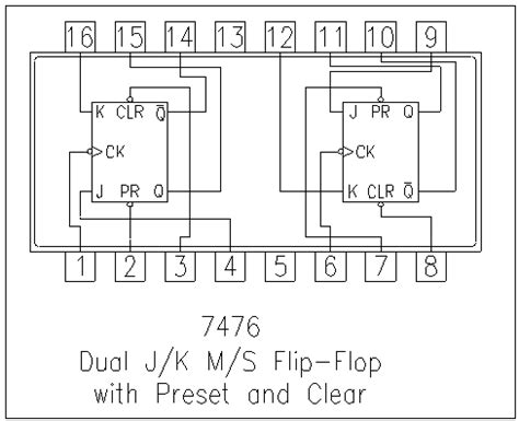
Pinout Diagram and Pin Descriptions
The 74LS76 comes in a 16-pin Dual In-Line Package (DIP). Here is the pinout diagram for the 74LS76:
| Pin | Symbol | Description |
|---|---|---|
| 1 | 1CLK | Clock input for flip-flop 1 |
| 2 | 1J | J input for flip-flop 1 |
| 3 | 1K | K input for flip-flop 1 |
| 4 | 1Q | Q output for flip-flop 1 |
| 5 | 1/Q | Complementary Q output for flip-flop 1 |
| 6 | 1/CLR | Active-low clear input for flip-flop 1 |
| 7 | 1/PRE | Active-low preset input for flip-flop 1 |
| 8 | GND | Ground |
| 9 | 2/CLR | Active-low clear input for flip-flop 2 |
| 10 | 2/PRE | Active-low preset input for flip-flop 2 |
| 11 | 2Q | Q output for flip-flop 2 |
| 12 | 2/Q | Complementary Q output for flip-flop 2 |
| 13 | 2K | K input for flip-flop 2 |
| 14 | 2J | J input for flip-flop 2 |
| 15 | 2CLK | Clock input for flip-flop 2 |
| 16 | VCC | Positive supply voltage (usually 5V) |
Let’s take a closer look at each pin and its function:
Clock Inputs (1CLK and 2CLK)
The clock inputs (1CLK for flip-flop 1 and 2CLK for flip-flop 2) are used to trigger the flip-flop operation. On the rising edge of the clock signal, the flip-flop samples the states of the J and K inputs and updates its outputs accordingly.
J and K Inputs (1J, 1K, 2J, 2K)
The J and K inputs determine the next state of the flip-flop outputs (Q and /Q) based on their logic levels at the rising edge of the clock signal. The behavior of the flip-flop depends on the combination of the J and K inputs:
| J | K | Flip-Flop Operation |
|---|---|---|
| 0 | 0 | No change |
| 0 | 1 | Reset (Q = 0, /Q = 1) |
| 1 | 0 | Set (Q = 1, /Q = 0) |
| 1 | 1 | Toggle (Q and /Q swap states) |
Q and /Q Outputs (1Q, 1/Q, 2Q, 2/Q)
The Q and /Q outputs represent the current state of the flip-flop. Q is the non-inverted output, while /Q is the inverted (complementary) output. The state of these outputs is determined by the J and K inputs at the rising edge of the clock signal, or by the preset and clear inputs.
Preset and Clear Inputs (1/PRE, 1/CLR, 2/PRE, 2/CLR)
The preset (PRE) and clear (CLR) inputs are active-low asynchronous inputs used to set or reset the flip-flop outputs independently of the clock signal. When the preset input is asserted low, the Q output is set to ‘1’ and /Q is set to ‘0’. When the clear input is asserted low, the Q output is reset to ‘0’ and /Q is set to ‘1’. If both preset and clear inputs are asserted simultaneously, the behavior is undefined.
Power Supply and Ground (VCC and GND)
The 74LS76 requires a power supply voltage (VCC) of typically 5V and a ground connection (GND) to operate properly. It is important to ensure that the power supply is stable and free from noise to avoid erratic behavior of the IC.
Timing Diagram and Operation
To better understand the operation of the 74LS76, let’s examine its timing diagram:
       _______________          _______________
1CLK
       _______________          _______________

         ___________
1J
         ___________

                 ___________
1K
                 ___________

                      ______
1Q
                      ______

                             ______
1/Q
                             ______

                                    _______
1/CLR
                                    _______

                                           ___
1/PRE
                                           ___
The timing diagram shows the relationship between the input signals and the resulting output states of the flip-flop. When the clock signal (CLK) transitions from low to high (rising edge), the flip-flop samples the states of the J and K inputs. Based on the sampled inputs, the Q and /Q outputs are updated according to the truth table mentioned earlier.
If the preset (PRE) input is asserted low, the Q output is set to ‘1’ and /Q is set to ‘0’ asynchronously, regardless of the clock signal. Similarly, if the clear (CLR) input is asserted low, the Q output is reset to ‘0’ and /Q is set to ‘1’ asynchronously.

Applications and Examples
The 74LS76 finds use in various digital circuits where storing and manipulating binary states is required. Some common applications include:
Counters
The 74LS76 can be used to build binary counters by cascading multiple flip-flops. By connecting the Q output of one flip-flop to the clock input of the next flip-flop, a ripple counter is formed. The J and K inputs can be used to control the counting sequence.
Example: 4-bit Binary Counter
           ___       ___       ___       ___
CLK -----|>CLK|-----|>CLK|-----|>CLK|-----|>CLK|
         |   |     |   |     |   |     |   |
         | J |     | J |     | J |     | J |
         |   |     |   |     |   |     |   |
         | K |     | K |     | K |     | K |
         |   |     |   |     |   |     |   |
          1Q        2Q        3Q        4Q
In this example, four 74LS76 flip-flops are cascaded to create a 4-bit binary counter. The J and K inputs of each flip-flop are tied to VCC (logic ‘1’) to enable toggling on each clock pulse. The Q outputs represent the binary count sequence.
Shift Registers
The 74LS76 can be configured as a shift register to store and shift binary data. By connecting the Q output of one flip-flop to the J input of the next flip-flop, data can be shifted through the register on each clock pulse.
Example: 4-bit Shift Register
        ___       ___       ___       ___
Data --|>J |-----|>J |-----|>J |-----|>J |
       |   |     |   |     |   |     |   |
       | K |     | K |     | K |     | K |
CLK ---|>CLK|-----|>CLK|-----|>CLK|-----|>CLK|
       |   |     |   |     |   |     |   |
        1Q        2Q        3Q        4Q
In this example, four 74LS76 flip-flops are connected to form a 4-bit shift register. The data is input to the J input of the first flip-flop, and on each clock pulse, the data is shifted from one flip-flop to the next. The Q outputs represent the shifted data.
Memory Elements
The 74LS76 can serve as a basic memory element to store a single bit of information. The preset and clear inputs can be used to initialize the memory state, while the J and K inputs can be used to update the stored data.
Example: 1-bit Memory
  Data ---|>J  |
          |    |
          |  K |
    CLK --|>CLK|
          |    |
  /CLR ---|>/CLR|
          |    |
  /PRE ---|>/PRE|
          |    |
           1Q
In this example, a single 74LS76 flip-flop is used as a 1-bit memory element. The data to be stored is connected to the J input, and the stored data is available at the Q output. The preset and clear inputs can be used to initialize the memory state, while the clock signal controls when the data is updated.

Frequently Asked Questions (FAQ)
1. What is the difference between the 74LS76 and other flip-flop ICs?
The 74LS76 is a dual J-K flip-flop with preset and clear inputs. It differs from other flip-flop ICs like the 74LS74 (dual D flip-flop) or the 74LS73 (dual J-K flip-flop with clear) in terms of the available inputs and the specific behavior of the flip-flop. The 74LS76 offers more control over the flip-flop’s operation with its J and K inputs, along with the asynchronous preset and clear functionality.
2. Can the 74LS76 be used as a toggle flip-flop?
Yes, the 74LS76 can be configured as a toggle flip-flop by connecting both the J and K inputs to VCC (logic ‘1’). In this configuration, the Q and /Q outputs will toggle their states on each rising edge of the clock signal.
3. What happens if the preset and clear inputs are asserted simultaneously?
If both the preset and clear inputs of the 74LS76 are asserted low simultaneously, the behavior of the flip-flop is undefined. It is important to ensure that the preset and clear inputs are not active at the same time to avoid unpredictable results.
4. Can the 74LS76 be used in synchronous circuits?
Yes, the 74LS76 can be used in synchronous circuits where the flip-flop’s operation is controlled by a clock signal. The J and K inputs are sampled on the rising edge of the clock, and the outputs are updated accordingly. However, it is important to note that the preset and clear inputs are asynchronous and can override the flip-flop’s state independently of the clock signal.
5. What is the maximum clock frequency that the 74LS76 can handle?
The maximum clock frequency that the 74LS76 can handle depends on various factors such as the supply voltage, output loading, and operating temperature. Typically, the 74LS76 can operate at clock frequencies up to around 25-30 MHz. However, for reliable operation, it is recommended to consult the device’s datasheet and adhere to the specified timing requirements and operating conditions.

Conclusion
The 74LS76 dual J-K flip-flop is a versatile IC that finds applications in various digital circuits such as counters, shift registers, and memory elements. Understanding the 74ls76 pinout and its functions is crucial for effectively utilizing this IC in your designs.
By exploring the pinout diagram, pin descriptions, timing diagram, and example applications, this comprehensive guide aims to provide a solid foundation for working with the 74LS76. Whether you are a beginner or an experienced electronics enthusiast, mastering the 74LS76 pinout will empower you to create robust and efficient digital circuits.
Remember to refer to the device’s datasheet for detailed specifications, timing requirements, and application notes specific to your design requirements. Happy designing with the 74LS76!
No responses yet