What are Printed Circuit Boards (PCBs)?
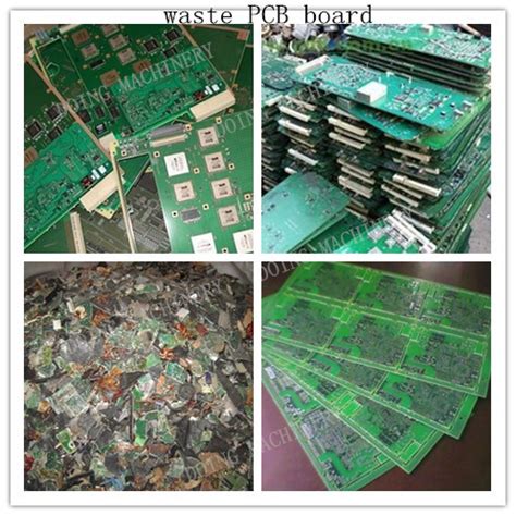
Printed circuit boards (PCBs) are the backbone of modern electronic devices. They are flat, thin boards made from a non-conductive material, such as fiberglass or plastic, with conductive pathways etched or printed onto the surface. These pathways, known as traces, connect various electronic components, such as resistors, capacitors, and integrated circuits, to form a functional electronic circuit. PCBs provide a compact and efficient means of assembling electronic devices, as they eliminate the need for individual wire connections between components.
The Importance of PCB Recycling
Environmental Impact
The rapid growth of e-waste has become a global environmental concern. According to the United Nations, the world generates approximately 50 million tonnes of e-waste annually, with only 20% being formally recycled. When improperly disposed of, e-waste can release harmful toxins and heavy metals into the environment, contaminating soil, water, and air. These pollutants can have severe consequences for human health and wildlife.
PCBs contain a variety of hazardous materials, such as lead, cadmium, and brominated flame retardants, which can leach into the environment if not properly handled. By recycling PCBs, we can prevent these harmful substances from polluting our ecosystems and protect the health of our planet.
Resource Conservation
PCBs contain valuable materials, such as precious metals (gold, silver, and palladium) and base metals (copper, aluminum, and tin). Recycling these materials helps conserve natural resources and reduces the need for mining and refining raw materials. This conservation effort not only protects the environment but also helps reduce the cost of manufacturing new electronic devices.
Economic Benefits
The e-waste recycling industry has the potential to create jobs and stimulate economic growth. As the demand for electronic devices continues to rise, so does the need for efficient and sustainable e-waste management solutions. By investing in PCB recycling infrastructure and technologies, countries can create new employment opportunities and boost their economies while addressing environmental concerns.

The PCB Recycling Process
The PCB recycling process involves several stages, each designed to maximize the recovery of valuable materials while minimizing environmental impact. The following steps outline the typical PCB recycling process:
1. Collection and Sorting
The first step in PCB recycling is the collection of e-waste from various sources, such as households, businesses, and e-waste drop-off centers. Once collected, the e-waste is sorted based on the type of device and the presence of hazardous materials. This sorting process helps streamline the recycling process and ensures that each type of e-waste receives the appropriate treatment.
2. Dismantling
After sorting, the electronic devices are manually dismantled to separate the PCBs from other components, such as plastic casings, batteries, and screens. This step is crucial in preventing contamination and ensuring the purity of the recovered materials.
3. Shredding
The separated PCBs are then shredded into smaller pieces, typically ranging from 1 to 5 cm in size. Shredding increases the surface area of the PCBs, making it easier to extract valuable materials in the subsequent stages of the recycling process.
4. Separation
The shredded PCBs undergo a series of separation processes to isolate the various materials based on their physical and chemical properties. Some common separation methods include:
- Magnetic separation: Ferrous metals, such as iron and steel, are removed using powerful magnets.
- Eddy current separation: Non-ferrous metals, such as aluminum and copper, are separated using a varying magnetic field that induces eddy currents in the metals, causing them to repel from the field.
- Density separation: Materials with different densities, such as plastics and metals, are separated using water or air separation techniques.
5. Refining
The separated materials are then refined to increase their purity and prepare them for reuse in the manufacturing of new products. Refining processes vary depending on the material being recovered, but some common methods include:
- Pyrometallurgy: This process involves heating the materials to high temperatures to extract and purify metals.
- Hydrometallurgy: This process uses aqueous solutions to extract and purify metals through leaching, solvent extraction, and electrowinning.
- Electrolysis: This process uses an electric current to separate and purify metals from a solution.

PCB Recycling Methods
There are several PCB recycling methods employed by e-waste recyclers worldwide. Each method has its advantages and disadvantages, and the choice of method depends on factors such as the type of PCBs being recycled, the available infrastructure, and the desired output. Some of the most common PCB recycling methods include:
Mechanical Recycling
Mechanical recycling is the most widely used method for PCB recycling. It involves shredding the PCBs into small pieces and then separating the materials using various physical separation techniques, such as magnetic separation, eddy current separation, and density separation. This method is relatively simple and cost-effective, but it may not achieve the highest purity of recovered materials compared to other methods.
Pyrometallurgical Recycling
Pyrometallurgical recycling involves heating the shredded PCBs to high temperatures in a smelting furnace to extract and purify metals. This method is particularly effective for recovering precious metals, such as gold and silver, but it can be energy-intensive and may generate harmful emissions if not properly controlled.
Hydrometallurgical Recycling
Hydrometallurgical recycling uses aqueous solutions to extract and purify metals from shredded PCBs. This method involves leaching the metals into a solution using acids or other chemicals, followed by solvent extraction and electrowinning to recover the purified metals. Hydrometallurgical recycling is more environmentally friendly than pyrometallurgical recycling, as it generates fewer emissions and requires less energy.
Biometallurgical Recycling
Biometallurgical recycling is an emerging technology that uses microorganisms, such as bacteria and fungi, to extract metals from PCBs. These microorganisms can selectively leach metals from the PCBs, making it easier to recover and purify them. Biometallurgical recycling is still in the research and development stage, but it shows promise as a sustainable and eco-friendly alternative to traditional recycling methods.

Challenges in PCB Recycling
Despite the numerous benefits of PCB recycling, there are several challenges that the industry faces:
Complexity of PCBs
PCBs are complex and diverse, with varying compositions and designs depending on the electronic device they are used in. This complexity makes it difficult to develop a standardized recycling process that can efficiently handle all types of PCBs.
Hazardous Materials
PCBs contain a range of hazardous materials, such as lead, cadmium, and brominated flame retardants, which can pose risks to human health and the environment if not properly handled during the recycling process. Recyclers must adhere to strict safety regulations and invest in specialized equipment to ensure the safe handling and disposal of these materials.
Lack of Infrastructure
In many countries, particularly in developing nations, there is a lack of proper e-waste recycling infrastructure. This deficiency can lead to the improper disposal of PCBs, which can have severe environmental and health consequences.
Economic Viability
The economic viability of PCB recycling depends on several factors, such as the cost of collection, transportation, and processing, as well as the market value of the recovered materials. Fluctuations in metal prices and the increasing complexity of PCBs can make it challenging for recyclers to maintain profitability.
Best Practices in PCB Recycling
To ensure the safe and efficient recycling of PCBs, it is essential to follow best practices throughout the recycling process. Some of these best practices include:
Proper Collection and Sorting
Establishing a well-organized collection and sorting system is crucial for the success of PCB recycling. E-waste should be collected from reliable sources and sorted based on the type of device and the presence of hazardous materials. Proper sorting helps prevent contamination and ensures that each type of e-waste receives the appropriate treatment.
Safe Handling of Hazardous Materials
Recyclers must implement strict safety protocols for handling hazardous materials found in PCBs. This includes providing proper personal protective equipment (PPE) for workers, using specialized containment systems to prevent the release of toxins, and adhering to local and international regulations for the disposal of hazardous waste.
Investment in Advanced Technologies
To improve the efficiency and effectiveness of PCB recycling, recyclers should invest in advanced technologies, such as automated sorting systems, high-precision shredders, and state-of-the-art refining equipment. These investments can help increase the recovery rate of valuable materials while reducing environmental impact and operational costs.
Collaboration and Knowledge Sharing
Collaboration and knowledge sharing among e-waste recyclers, researchers, and policymakers are essential for advancing the PCB recycling industry. By working together to develop new technologies, establish best practices, and create supportive policies, we can build a more sustainable and efficient e-waste management system.
The Future of PCB Recycling
As the world becomes increasingly digitized, the volume of e-waste, including PCBs, is expected to continue growing. To address this challenge, the PCB recycling industry must adapt and innovate. Some of the key trends and developments shaping the future of PCB recycling include:
Circular Economy
The concept of a circular economy, in which resources are kept in use for as long as possible through reuse, recycling, and remanufacturing, is gaining traction in the e-waste management sector. By designing electronic products with recycling in mind and establishing closed-loop recycling systems, we can minimize waste and maximize resource efficiency.
Advanced Recycling Technologies
Researchers and innovators are continuously developing new technologies to improve the efficiency and sustainability of PCB recycling. Some promising advancements include the use of robotics and artificial intelligence for automated sorting, the development of more eco-friendly leaching agents for hydrometallurgical recycling, and the application of biometallurgy for metal recovery.
Policy and Regulation
Governments and international organizations play a crucial role in shaping the future of PCB recycling through policy and regulation. By implementing stringent e-waste management laws, setting recycling targets, and providing incentives for sustainable practices, policymakers can drive the growth of the PCB recycling industry and ensure its environmental and social responsibility.
Consumer Awareness
Increasing consumer awareness about the importance of e-waste recycling is essential for the success of the PCB recycling industry. By educating the public about the environmental and health impacts of improper e-waste disposal and providing accessible recycling options, we can encourage more people to participate in responsible e-waste management practices.
Frequently Asked Questions (FAQ)
-
Q: What are the most valuable materials found in PCBs?
A: The most valuable materials found in PCBs are precious metals, such as gold, silver, and palladium, and base metals, such as copper, aluminum, and tin. -
Q: Can all types of PCBs be recycled?
A: While most PCBs can be recycled, some types may be more challenging to process due to their complexity or the presence of certain hazardous materials. However, with the right technologies and processes, the majority of PCBs can be effectively recycled. -
Q: How can I responsibly dispose of my old electronic devices containing PCBs?
A: To responsibly dispose of your old electronic devices, look for certified e-waste recyclers in your area. Many cities and towns have e-waste collection events or drop-off centers where you can bring your devices for proper recycling. -
Q: Are there any health risks associated with PCB recycling?
A: If proper safety measures are not followed, PCB recycling can pose health risks to workers and the environment due to the presence of hazardous materials. However, reputable recyclers adhere to strict safety regulations and use specialized equipment to minimize these risks. -
Q: How can I support the growth of the PCB recycling industry?
A: You can support the growth of the PCB recycling industry by properly disposing of your e-waste, spreading awareness about the importance of e-waste recycling, and supporting businesses and organizations that prioritize sustainable e-waste management practices.
Conclusion
PCB recycling is a critical process in the sustainable management of e-waste, offering numerous environmental, economic, and social benefits. As the world becomes increasingly reliant on electronic devices, it is essential that we develop efficient and responsible recycling practices to minimize the negative impacts of e-waste on our planet and its inhabitants.
By understanding the various methods and best practices involved in PCB recycling, and by staying informed about the latest developments and trends in the industry, we can all contribute to building a more sustainable future. Through collaboration, innovation, and commitment, we can transform the challenge of e-waste into an opportunity for positive change, ensuring that the benefits of technology are enjoyed by generations to come without compromising the health of our environment.
| Material | Percentage in PCBs |
|---|---|
| Copper | 15-20% |
| Fiberglass | 50-70% |
| Tin | 3-5% |
| Lead | 2-5% |
| Nickel | 1-3% |
| Gold | 0.05-0.1% |
| Silver | 0.01-0.05% |
| Palladium | 0.005-0.01% |
This table provides an overview of the typical composition of PCBs, highlighting the percentage of various materials found in these boards. Understanding the composition of PCBs is crucial for developing effective recycling processes and maximizing the recovery of valuable materials.
No responses yet