What is PCB Solderability?
PCB solderability refers to the ability of the printed circuit board’s surface to be wetted by molten solder and form a strong mechanical and electrical bond. Good solderability is crucial for ensuring reliable connections between components and the PCB. Poor solderability can lead to weak joints, open circuits, and other defects that compromise the functionality and durability of the assembled board.
Factors Affecting PCB Solderability
Several factors can influence the solderability of a PCB:
-
Surface finish: The type of surface finish applied to the PCB pads and holes, such as HASL, ENIG, or OSP, affects how well the solder adheres to the surface.
-
Storage conditions: Exposure to humidity, high temperatures, or contaminants during storage can degrade the solderability of the PCB over time.
-
Age of the PCB: As the PCB ages, the surface finish may oxidize or deteriorate, reducing its ability to be wetted by solder.
-
Design and manufacturing quality: Proper design and manufacturing practices, such as appropriate pad sizes and shapes, hole plating, and cleanliness, contribute to good solderability.
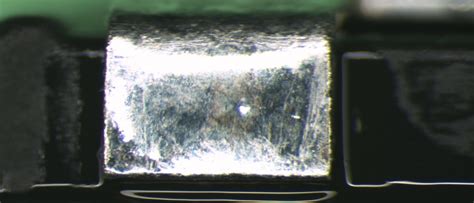
PCB Solderability Testing Methods
To ensure that PCBs meet the required solderability standards, various testing methods are employed:
Wetting Balance Test
The wetting balance test measures the wetting force and time of a solder meniscus on a test coupon. A sample PCB is dipped into a solder bath, and the force exerted by the meniscus is recorded over time. This test provides quantitative data on the wetting properties of the surface finish.
Dip and Look Test
In the dip and look test, a sample PCB is dipped into a solder bath for a specified time and then visually inspected for the presence and quality of the solder coating. This qualitative test is quick and simple but relies on the judgment of the operator.
Edge Dip Test
The edge dip test involves dipping the edge of a sample PCB into a solder bath at a 45-degree angle. After a specified time, the sample is removed and examined for the presence and extent of the solder coating. This test is useful for evaluating the solderability of PCB edges and corners.
Hole Fill Test
The hole fill test assesses the ability of molten solder to fill the plated through-holes of a PCB. A sample board is floated on a solder bath, and the percentage of hole fill is evaluated using X-ray imaging or microsectioning. This test is essential for ensuring reliable through-hole connections.

Interpreting Solderability Test Results
Solderability test results are typically evaluated against industry standards, such as IPC-J-STD-003, which define acceptable criteria for wetting time, wetting force, and solder coverage. The following table summarizes some common acceptance criteria:
| Test Method | Acceptance Criteria |
|---|---|
| Wetting Balance Test | Wetting time: ≤2 seconds Wetting force: ≥2.5 mN/mm |
| Dip and Look Test | Solder coverage: ≥95% of tested surface area |
| Edge Dip Test | Solder coverage: ≥95% of tested edge length |
| Hole Fill Test | Hole fill: ≥75% of hole depth |
Meeting these criteria indicates that the PCB has good solderability and is likely to produce reliable solder joints during assembly.

Maintaining PCB Solderability
To maintain the solderability of PCBs throughout their shelf life, it is important to follow proper storage and handling procedures:
-
Moisture control: Store PCBs in a dry environment with relative humidity below 60% to prevent oxidation and degradation of the surface finish.
-
Temperature control: Avoid exposing PCBs to high temperatures, which can accelerate the aging of the surface finish. Store boards at room temperature or below.
-
Packaging: Use moisture-barrier bags with desiccants to protect PCBs from humidity during storage and transportation.
-
Handling: Minimize manual handling of PCBs to reduce the risk of contamination. Use gloves or finger cots when handling boards.
-
Shelf life management: Track the age of PCBs and use older boards first to avoid excessive aging. Follow the manufacturer’s recommended shelf life for each surface finish type.

Frequently Asked Questions (FAQ)
1. What is the difference between HASL and ENIG surface finishes in terms of solderability?
HASL (Hot Air Solder Leveling) and ENIG (Electroless Nickel Immersion Gold) are two common surface finishes used on PCBs. HASL involves dipping the board in molten solder and then blowing off the excess, resulting in a tin-lead coating. ENIG consists of a nickel layer topped with a thin gold layer, providing a flat and solderable surface.
In terms of solderability, both HASL and ENIG perform well, but ENIG has some advantages:
- ENIG provides a flatter surface, which is beneficial for fine-pitch components.
- ENIG has a longer shelf life than HASL, as the gold layer protects the nickel from oxidation.
- ENIG is lead-free, making it more environmentally friendly and compliant with RoHS regulations.
However, HASL is often preferred for its lower cost and compatibility with a wider range of solder alloys.
2. Can poor solderability cause tombstoning of surface mount components?
Yes, poor solderability can contribute to tombstoning, also known as drawbridging, of surface mount components. Tombstoning occurs when one end of a component lifts off the PCB pad during reflow soldering, resulting in an open circuit.
Several factors related to solderability can increase the risk of tombstoning:
- Uneven solder paste deposition or wetting on the pads
- Misalignment of the component or pads
- Differences in solderability between the component leads and PCB pads
- Inappropriate reflow temperature profile or ramp rates
To minimize tombstoning, ensure that the PCB and components have good solderability, use proper solder paste and stencil design, and optimize the reflow soldering process.
3. How often should PCB solderability be tested?
The frequency of PCB solderability testing depends on several factors, such as the PCB’s surface finish, storage conditions, and intended use. In general, it is recommended to test solderability:
- Before assembling the PCBs, especially if they have been stored for an extended period
- After any changes to the PCB manufacturing process or materials
- Periodically during storage to monitor the aging of the surface finish
For critical applications or long-term storage, solderability testing may be performed more frequently, such as every 3-6 months. It is essential to establish a testing plan based on the specific requirements and risks associated with the PCBs.
4. Can solderability be improved on aged or oxidized PCBs?
In some cases, solderability can be improved on aged or oxidized PCBs through a process called solder dipping or hot solder leveling. This involves dipping the affected areas of the PCB into molten solder to remove the oxidized layer and deposit a fresh solder coating.
However, solder dipping has limitations and risks:
- It may not be effective for severely oxidized or contaminated surfaces
- The high temperature of the molten solder can cause thermal stress or damage to the PCB
- The process may affect the dimensional accuracy of the PCB features
- Rework may be required to remove excess solder or address any resulting defects
Before attempting to improve solderability through solder dipping, it is essential to assess the condition of the PCBs and consider the potential risks and benefits. In some cases, it may be more cost-effective to replace the PCBs with fresher ones.
5. What role does cleanliness play in PCB solderability?
Cleanliness is a critical factor in maintaining good PCB solderability. Contaminants on the PCB surface, such as flux residues, oils, or dust, can interfere with the wetting and spreading of solder, leading to poor joint quality or solderability issues.
To ensure cleanliness and good solderability, follow these practices:
- Use clean and compatible materials during PCB fabrication and assembly
- Implement proper cleaning processes to remove any residues or contaminants
- Handle PCBs in a clean environment, using gloves or finger cots to avoid introducing oils or moisture
- Store PCBs in sealed, moisture-barrier packaging with desiccants to prevent contamination during storage and transportation
- Monitor the cleanliness of PCBs through visual inspection or analytical techniques, such as ion chromatography or surface insulation resistance testing
By maintaining a high level of cleanliness throughout the PCB manufacturing and assembly process, you can minimize solderability issues and ensure more reliable and consistent solder joint quality.
Conclusion
PCB solderability is a critical aspect of ensuring reliable and functional electronic assemblies. By understanding the factors that influence solderability, employing appropriate testing methods, and following best practices for storage and handling, manufacturers can maintain the solderability of their PCBs throughout their shelf life. Regular solderability testing and monitoring, combined with proper design and manufacturing processes, can help identify and prevent solderability issues before they lead to assembly defects or field failures. As the electronics industry continues to evolve, with increasing component density and complexity, maintaining good PCB solderability will remain a key priority for ensuring the quality and reliability of electronic products.
Word count: 1506 words
No responses yet