Introduction to Gold Finger PCBs
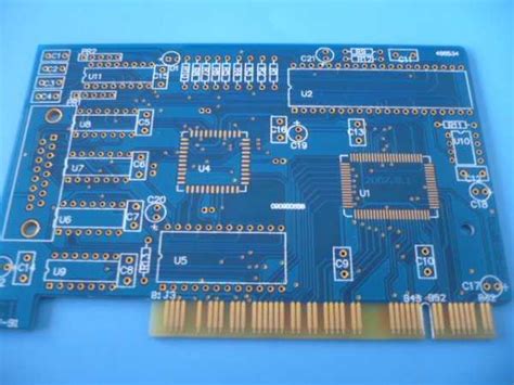
Gold finger PCBs, also known as edge connector PCBs or gold-plated edge connectors, are specialized printed circuit boards designed with gold-plated contact fingers along one edge. These gold fingers provide a reliable and durable connection interface for connecting PCBs to other devices or components. Gold finger PCBs are commonly used in various applications, such as computer peripherals, communication systems, and industrial equipment.
What are Gold Finger PCBs?
Gold finger PCBs are printed circuit boards that feature gold-plated contact pads or fingers along one edge of the board. These gold fingers are designed to mate with corresponding connectors or slots, allowing the PCB to establish an electrical and mechanical connection with other devices or components. The gold plating on the contact fingers ensures excellent conductivity, corrosion resistance, and durability.
Benefits of Gold Finger PCBs
Gold finger PCBs offer several advantages over other connection methods:
- Reliability: Gold-plated contacts provide a reliable and stable connection, even in harsh environments or under frequent insertion and removal cycles.
- Durability: The gold plating on the contact fingers is resistant to corrosion, oxidation, and wear, ensuring a long-lasting connection.
- High conductivity: Gold is an excellent conductor of electricity, ensuring low contact resistance and efficient signal transmission.
- Ease of use: Gold finger PCBs can be easily inserted into and removed from corresponding connectors or slots, simplifying the assembly and maintenance process.
Types of Gold Finger PCBs
There are several types of gold finger PCBs, each designed for specific applications and requirements.
Single-Sided Gold Finger PCBs
Single-sided gold finger PCBs have gold-plated contact fingers on only one side of the board. These PCBs are commonly used in applications where the connection is made from only one side, such as in expansion cards or module interfaces.
Double-Sided Gold Finger PCBs
Double-sided gold finger PCBs have gold-plated contact fingers on both sides of the board. These PCBs are suitable for applications that require a higher number of connections or when the PCB needs to be inserted into a connector from either side.
Hybrid Gold Finger PCBs
Hybrid gold finger PCBs combine gold-plated contact fingers with other connection methods, such as surface mount technology (SMT) or through-hole components. These PCBs offer the benefits of gold finger connectivity while accommodating other components and circuitry on the same board.
Comparison of Gold Finger PCB Types
| Type | Sides with Gold Fingers | Typical Applications |
|---|---|---|
| Single-Sided Gold Finger | One | Expansion cards, module interfaces |
| Double-Sided Gold Finger | Two | High-density connections, dual-side insertion |
| Hybrid Gold Finger | One or Two | Combined with SMT or through-hole components |

Manufacturing Process of Gold Finger PCBs
The manufacturing process of gold finger PCBs involves several key steps to ensure the quality and reliability of the final product.
PCB Fabrication
The first step in manufacturing gold finger PCBs is the fabrication of the base PCB. This process involves:
- Designing the PCB layout and circuitry using CAD software
- Printing the circuit pattern onto the copper-clad laminate
- Etching away the unwanted copper to create the desired traces and pads
- Drilling holes for through-hole components (if required)
Gold Plating
After the base PCB is fabricated, the gold plating process is carried out on the contact fingers. This process typically involves:
- Cleaning the contact fingers to remove any contaminants or oxides
- Applying a nickel underlayer to provide a barrier between the copper and gold layers
- Electroplating a layer of gold onto the nickel underlayer
- Inspecting the gold-plated fingers for thickness, uniformity, and any defects
Solder Mask Application
A solder mask is applied to the PCB to protect the copper traces and pads from oxidation and short-circuits. The solder mask is selectively applied, leaving the gold-plated fingers exposed for connection.
Surface Finish
The exposed copper areas on the PCB, such as component pads and test points, are often coated with a surface finish to prevent oxidation and improve solderability. Common surface finishes for gold finger PCBs include:
- Hot Air Solder Leveling (HASL)
- Electroless Nickel Immersion Gold (ENIG)
- Immersion Silver (IAg)
- Immersion Tin (ISn)
Quality Control
Throughout the manufacturing process, strict quality control measures are implemented to ensure the reliability and performance of the gold finger PCBs. This includes:
- Visual inspection for any defects or anomalies
- Electrical testing to verify continuity and insulation resistance
- Mechanical testing to ensure the durability and stability of the gold-plated fingers
- Conformance to industry standards and customer specifications

Design Considerations for Gold Finger PCBs
When designing gold finger PCBs, several key factors must be considered to ensure optimal performance and reliability.
Contact Finger Dimensions
The dimensions of the gold-plated contact fingers, such as width, pitch, and length, must be carefully designed to mate properly with the corresponding connector or slot. Industry standards, such as PCI Express or CompactPCI, provide guidelines for contact finger dimensions.
Gold Plating Thickness
The thickness of the gold plating on the contact fingers is a critical factor in determining the durability and performance of the connection. Typically, a gold plating thickness of 30 microinches (0.76 micrometers) or more is recommended for reliable and long-lasting connections.
Impedance Control
For high-speed and high-frequency applications, impedance control is essential to maintain signal integrity and minimize reflections. The PCB layout and stack-up must be designed to achieve the desired characteristic impedance of the traces and gold fingers.
Mechanical Stability
The mechanical stability of the gold finger PCB is crucial for maintaining a reliable connection under repeated insertion and removal cycles. Factors such as board thickness, copper weight, and laminate material selection contribute to the overall mechanical stability of the PCB.
Solder Mask Clearance
The solder mask clearance around the gold-plated fingers must be carefully designed to prevent solder bridging or contamination during the assembly process. Adequate clearance ensures that the gold fingers remain exposed and accessible for connection.

Applications of Gold Finger PCBs
Gold finger PCBs find applications in various industries and products where reliable and durable connections are essential.
Computer Peripherals
Gold finger PCBs are commonly used in computer peripherals, such as:
- Graphics cards
- Sound cards
- Network interface cards (NICs)
- Memory modules (e.g., DIMM, SIMM)
Communication Systems
In communication systems, gold finger PCBs are used for:
- Backplane connectors
- Mezzanine cards
- Daughterboards
- Modular transceivers
Industrial Equipment
Industrial equipment often relies on gold finger PCBs for robust and reliable connections in:
- Programmable logic controllers (PLCs)
- Industrial PCs
- Embedded systems
- Data acquisition modules
Consumer Electronics
Gold finger PCBs are also used in consumer electronics products, such as:
- Game cartridges
- Smartphone and tablet expansion modules
- Digital cameras
- Portable audio devices
FAQ
1. What is the difference between gold finger PCBs and regular PCBs?
Gold finger PCBs have gold-plated contact fingers along one edge of the board, providing a reliable and durable connection interface. Regular PCBs may not have gold-plated fingers and rely on other connection methods, such as connectors or solder joints.
2. Why is gold used for plating the contact fingers?
Gold is used for plating the contact fingers due to its excellent conductivity, corrosion resistance, and durability. Gold-plated contacts provide a reliable and stable connection, even under frequent insertion and removal cycles or in harsh environments.
3. How thick should the gold plating be on the contact fingers?
A gold plating thickness of 30 microinches (0.76 micrometers) or more is typically recommended for reliable and long-lasting connections. However, the specific thickness requirement may vary depending on the application and industry standards.
4. Can gold finger PCBs be used for high-speed or high-frequency applications?
Yes, gold finger PCBs can be designed for high-speed and high-frequency applications. Proper impedance control, PCB layout, and stack-up design are essential to maintain signal integrity and minimize reflections in such applications.
5. How can I ensure the mechanical stability of gold finger PCBs?
To ensure the mechanical stability of gold finger PCBs, consider factors such as board thickness, copper weight, and laminate material selection. Proper design and manufacturing processes, along with adherence to industry standards, contribute to the overall mechanical stability of the PCB.
Conclusion
Gold finger PCBs offer a reliable and durable solution for connecting PCBs to other devices or components. With their gold-plated contact fingers, these specialized PCBs provide excellent conductivity, corrosion resistance, and mechanical stability. By understanding the types, manufacturing process, design considerations, and applications of gold finger PCBs, engineers and designers can effectively incorporate them into their projects to achieve optimal performance and reliability.
As technology advances and the demand for robust and high-performance connections grows, gold finger PCBs will continue to play a crucial role in various industries, from computer peripherals and communication systems to industrial equipment and consumer electronics.
No responses yet