What is PCB Tenting?
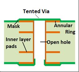
PCB tenting, also known as via tenting or tented vias, is a process used in the manufacturing of printed circuit boards (PCBs) where the drilled holes (vias) on the board are covered with a thin layer of solder mask material. This process is crucial in ensuring the reliability and functionality of the PCB.
Tenting vias helps to protect the vias from environmental factors such as dust, moisture, and other contaminants that could potentially damage the circuitry. It also prevents solder from flowing into the vias during the soldering process, which can cause short circuits and other issues.
Why is PCB Tenting Important?
PCB tenting is an essential process in PCB manufacturing for several reasons:
1. Protection from Environmental Factors
One of the primary reasons for using PCB tenting is to protect the vias from environmental factors such as dust, moisture, and other contaminants. These factors can cause corrosion, short circuits, and other issues that can affect the functionality and reliability of the PCB.
By covering the vias with a layer of solder mask material, PCB tenting creates a barrier that prevents these environmental factors from coming into contact with the exposed metal surfaces of the vias. This helps to ensure that the PCB remains functional and reliable over its intended lifespan.
2. Prevention of Solder Bridging
Another important reason for using PCB tenting is to prevent solder from flowing into the vias during the soldering process. When solder flows into the vias, it can create short circuits and other issues that can affect the functionality of the PCB.
PCB tenting helps to prevent this by creating a barrier that prevents the solder from flowing into the vias. This ensures that the solder only flows where it is intended to go, which helps to maintain the integrity of the PCB’s electrical connections.
3. Improved Signal Integrity
PCB tenting can also help to improve the signal integrity of the PCB. When vias are left exposed, they can act as tiny antennas that can pick up electromagnetic interference (EMI) from nearby components or external sources. This can cause signal distortion and other issues that can affect the performance of the PCB.
By covering the vias with a layer of solder mask material, PCB tenting helps to reduce the amount of EMI that can penetrate the vias. This helps to maintain the integrity of the signals passing through the PCB, which is especially important in high-speed or high-frequency applications.
4. Improved Manufacturability
PCB tenting can also help to improve the manufacturability of the PCB. When vias are left exposed, they can be difficult to clean and inspect during the manufacturing process. This can lead to defects and other issues that can affect the quality and reliability of the finished product.
By covering the vias with a layer of solder mask material, PCB tenting makes it easier to clean and inspect the PCB during the manufacturing process. This helps to ensure that the finished product meets the required quality standards and is free from defects.

Types of PCB Tenting
There are two main types of PCB tenting: full tenting and partial tenting.
1. Full Tenting
Full tenting, also known as complete tenting, is a process where the entire via is covered with a layer of solder mask material. This creates a complete barrier that prevents environmental factors and solder from coming into contact with the exposed metal surfaces of the via.
Full tenting is typically used in applications where maximum protection is required, such as in harsh environmental conditions or in high-reliability applications.
2. Partial Tenting
Partial tenting, also known as selective tenting, is a process where only a portion of the via is covered with a layer of solder mask material. This creates a partial barrier that allows some exposure of the metal surfaces of the via.
Partial tenting is typically used in applications where some exposure of the via is acceptable, such as in low-cost or low-reliability applications. It can also be used in situations where full tenting is not possible due to design constraints or other factors.

Advantages and Disadvantages of PCB Tenting
Like any manufacturing process, PCB tenting has its advantages and disadvantages. Here are some of the main pros and cons of using PCB tenting:
Advantages
- Protection from environmental factors
- Prevention of solder bridging
- Improved signal integrity
- Improved manufacturability
- Increased reliability and longevity of the PCB
Disadvantages
- Increased cost and complexity of the manufacturing process
- Potential for defects or issues if not performed correctly
- Limitations on the size and spacing of vias that can be tented
- Potential for reduced thermal dissipation in some applications

PCB Tenting Design Considerations
When designing a PCB that will use tenting, there are several factors to consider to ensure the best possible results. Here are some of the main design considerations for PCB tenting:
1. Via Size and Spacing
The size and spacing of the vias on the PCB can have a significant impact on the effectiveness of the tenting process. Smaller vias and tighter spacing can make it more difficult to achieve a consistent and reliable tenting layer.
When designing a PCB for tenting, it is important to follow the manufacturer’s guidelines for via size and spacing to ensure the best possible results. In general, larger vias and wider spacing will make it easier to achieve a consistent and reliable tenting layer.
2. Solder Mask Material
The choice of solder mask material can also have a significant impact on the effectiveness of the tenting process. Different materials have different properties and characteristics that can affect the adhesion, durability, and performance of the tenting layer.
When selecting a solder mask material for PCB tenting, it is important to consider factors such as the operating temperature range, the environmental conditions, and the required level of protection. Some common solder mask materials used for PCB tenting include liquid photoimageable (LPI) solder mask, dry film solder mask, and spray-on solder mask.
3. Tenting Method
The tenting method used can also have a significant impact on the effectiveness of the tenting process. There are several different methods that can be used to apply the solder mask material to the PCB, each with its own advantages and disadvantages.
Some common tenting methods include screen printing, spraying, and dipping. The choice of method will depend on factors such as the size and complexity of the PCB, the required level of protection, and the available equipment and expertise.
PCB Tenting Testing and Inspection
To ensure the quality and reliability of the tenting process, it is important to perform thorough testing and inspection of the PCB. Here are some of the main testing and inspection methods used for PCB tenting:
1. Visual Inspection
Visual inspection is the most basic method of testing and inspecting PCB tenting. This involves visually examining the PCB under magnification to check for any defects or issues with the tenting layer.
Common defects to look for include voids, bubbles, cracks, and inconsistencies in the thickness or coverage of the tenting layer. Visual inspection can be performed manually or using automated optical inspection (AOI) equipment.
2. Electrical Testing
Electrical testing is used to verify the functionality and performance of the PCB after tenting. This involves applying electrical signals to the PCB and measuring the response to ensure that the tenting layer is not affecting the electrical properties of the board.
Common electrical tests used for PCB tenting include continuity testing, insulation resistance testing, and high-potential (hipot) testing. These tests can help to identify any short circuits, open circuits, or other issues that may be caused by defects in the tenting layer.
3. Environmental Testing
Environmental testing is used to evaluate the durability and reliability of the PCB tenting under different environmental conditions. This involves exposing the PCB to various environmental stresses such as temperature, humidity, and vibration to ensure that the tenting layer remains intact and functional.
Common environmental tests used for PCB tenting include thermal cycling, humidity testing, and salt spray testing. These tests can help to identify any weaknesses or vulnerabilities in the tenting layer that may affect the long-term reliability of the PCB.
PCB Tenting Standards and Certifications
To ensure the quality and consistency of PCB tenting, there are several industry standards and certifications that manufacturers can follow. Here are some of the main standards and certifications used for PCB tenting:
1. IPC Standards
The IPC (Association Connecting Electronics Industries) is a global trade association that develops and publishes standards for the electronics industry. There are several IPC standards that relate to PCB tenting, including:
- IPC-A-600: Acceptability of Printed Boards
- IPC-6012: Qualification and Performance Specification for Rigid Printed Boards
- IPC-SM-840: Qualification and Performance of Permanent Solder Mask
These standards provide guidelines and requirements for the design, fabrication, and testing of PCBs with tented vias.
2. UL Certification
UL (Underwriters Laboratories) is a global safety certification company that provides testing and certification services for a wide range of products, including PCBs. UL offers several certifications related to PCB tenting, including:
- UL 94: Standard for Safety of Flammability of Plastic Materials for Parts in Devices and Appliances
- UL 746: Standard for Safety of Polymeric Materials – Use in Electrical Equipment Evaluations
These certifications provide assurance that the PCB tenting material meets specific safety and performance requirements.
FAQ
1. What is the difference between full tenting and partial tenting?
Full tenting involves covering the entire via with solder mask material, while partial tenting only covers a portion of the via. Full tenting provides maximum protection from environmental factors and solder bridging, while partial tenting allows some exposure of the via and may be used in low-cost or low-reliability applications.
2. Can PCB tenting be used on all types of PCBs?
PCB tenting can be used on most types of PCBs, including rigid, flexible, and rigid-flex boards. However, the effectiveness of the tenting process may vary depending on the size, spacing, and location of the vias, as well as the choice of solder mask material and tenting method.
3. How does PCB tenting affect the cost of the manufacturing process?
PCB tenting can increase the cost and complexity of the manufacturing process, as it requires additional materials, equipment, and labor compared to non-tented PCBs. However, the benefits of tenting, such as improved reliability and protection from environmental factors, may outweigh the additional cost in many applications.
4. What are some common defects to look for in PCB tenting?
Common defects in PCB tenting include voids, bubbles, cracks, and inconsistencies in the thickness or coverage of the tenting layer. These defects can be caused by issues with the solder mask material, the tenting method, or the PCB design, and can affect the functionality and reliability of the PCB.
5. What environmental factors can affect the durability of PCB tenting?
Environmental factors such as temperature, humidity, and vibration can all affect the durability and reliability of PCB tenting. Exposure to high temperatures or humidity can cause the tenting layer to degrade or delaminate, while vibration can cause cracks or other mechanical damage. Proper environmental testing can help to identify and mitigate these issues.
Conclusion
PCB tenting is a critical process in the manufacturing of printed circuit boards, providing protection from environmental factors, prevention of solder bridging, improved signal integrity, and increased reliability and longevity of the PCB. When designing a PCB for tenting, it is important to consider factors such as via size and spacing, solder mask material, and tenting method to ensure the best possible results.
Thorough testing and inspection, including visual inspection, electrical testing, and environmental testing, can help to identify and mitigate any defects or issues with the tenting layer. Following industry standards and certifications, such as IPC and UL, can also help to ensure the quality and consistency of PCB tenting.
While PCB tenting can increase the cost and complexity of the manufacturing process, the benefits it provides in terms of reliability, protection, and performance make it a valuable investment for many applications. As PCB technology continues to advance, the importance of PCB tenting will only continue to grow, making it a critical consideration for anyone involved in the design and manufacture of printed circuit boards.
No responses yet