What is a 2N222 Transistor?
The 2N222 is an NPN BJT designed for low-power applications. It is capable of handling a maximum collector current of 600mA and a maximum collector-emitter voltage of 40V. The transistor is commonly used in switching circuits, amplifiers, and as a general-purpose transistor in various electronic projects.
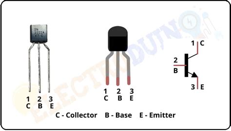
2N222 Pinout Configuration
The 2N222 transistor has three pins: the emitter (E), base (B), and collector (C). The pinout configuration is as follows:
| Pin | Symbol | Description |
|---|---|---|
| 1 | E | Emitter |
| 2 | B | Base |
| 3 | C | Collector |
Here’s a visual representation of the 2N222 pinout:
      +-----+
      |     |
      |  B  |
      |     |
 E ---+     +--- C
      |     |
      |     |
      +-----+
Emitter (E)
The emitter is the pin from which current flows out of the transistor when it is in the forward active mode. In an NPN transistor like the 2N222, the emitter is typically connected to the ground or the negative supply voltage.
Base (B)
The base is the control pin of the transistor. A small current flowing into the base allows a much larger current to flow from the collector to the emitter. The base current determines the amount of collector current that can flow through the transistor.
Collector (C)
The collector is the pin through which current enters the transistor when it is in the forward active mode. In an NPN transistor, the collector is typically connected to the positive supply voltage through a load.

2N222 Characteristics and Specifications
To effectively use the 2N222 transistor in your projects, it’s important to understand its key characteristics and specifications. Here are some of the most important parameters:
| Parameter | Value |
|---|---|
| Maximum Collector-Emitter Voltage | 40V |
| Maximum Collector Current | 600mA |
| Maximum Power Dissipation | 500mW |
| DC Current Gain (hFE) | 100-300 |
| Transition Frequency (fT) | 250MHz |
| Maximum Operating Temperature | 150°C |
These specifications provide a guideline for the safe and optimal operation of the 2N222 transistor. It’s crucial to ensure that your circuit design stays within these limits to prevent damage to the transistor and ensure reliable performance.

2N222 Applications
The 2N222 transistor finds applications in a wide range of electronic circuits. Some common uses include:
-
Switching Circuits: The 2N222 can be used as a switch to control the flow of current in a circuit. It can be used to turn devices on and off, such as LEDs, relays, or motors.
-
Amplifiers: The 2N222 can be employed in small-signal amplifier circuits to amplify weak signals. It is suitable for use in audio amplifiers, signal conditioning circuits, and preamplifiers.
-
Logic Gates: By combining multiple 2N222 transistors, you can create basic logic gates like AND, OR, and NOT gates. These gates form the building blocks of digital circuits.
-
Current Limiting: The 2N222 can be used as a current limiter to protect sensitive components from excessive current. By controlling the base current, you can limit the maximum collector current.
-
Oscillators: The 2N222 can be used in oscillator circuits to generate periodic waveforms. It can be configured in various oscillator topologies, such as the Colpitts oscillator or the Hartley oscillator.

2N222 Biasing and Circuit Design Considerations
To ensure proper operation of the 2N222 transistor in your circuits, it’s essential to consider biasing and other design factors. Here are some key points to keep in mind:
-
Base Resistor: When using the 2N222 as a switch or an amplifier, a base resistor is typically required to limit the base current and prevent excessive current flow. The value of the base resistor depends on the desired collector current and the transistor’s DC current gain (hFE).
-
Collector Resistor: The collector resistor determines the collector current and the voltage drop across the transistor. Its value should be chosen based on the desired collector current and the supply voltage.
-
Heat Dissipation: Like all transistors, the 2N222 generates heat during operation. It’s important to ensure that the power dissipation stays within the specified limit (500mW) to prevent damage to the transistor. In high-power applications, proper heat sinking may be necessary.
-
Input and Output Impedance: When designing amplifier circuits, consider the input and output impedance of the transistor. The 2N222 has a relatively low input impedance, which may require impedance matching techniques for optimal performance.
-
Gain and Frequency Response: The 2N222 has a DC current gain (hFE) ranging from 100 to 300 and a transition frequency (fT) of 250MHz. These parameters influence the amplification and frequency response of the transistor in your circuit.
Frequently Asked Questions (FAQ)
-
Q: Can I replace a 2N2222 transistor with a 2N222?
A: While the 2N222 and 2N2222 are both NPN BJTs, they have slightly different specifications. The 2N2222 has a higher maximum collector current rating (800mA) compared to the 2N222 (600mA). In most cases, you can use a 2N2222 as a substitute for a 2N222, but not vice versa. Always refer to the specific device datasheets for accurate specifications. -
Q: How do I test a 2N222 transistor?
A: To test a 2N222 transistor, you can use a multimeter in the diode test mode. Connect the black probe to the emitter and the red probe to the base and collector separately. A properly functioning NPN transistor should show a voltage drop of around 0.6V-0.7V between the base and emitter, and the base and collector. Swap the probes, and the multimeter should display an open circuit (OL) in both cases. -
Q: What is the maximum power dissipation of a 2N222 transistor?
A: The maximum power dissipation of a 2N222 transistor is 500mW. This value represents the maximum amount of power the transistor can safely dissipate without damage. Exceeding this limit can lead to overheating and permanent damage to the device. -
Q: How do I determine the base resistor value for a 2N222 transistor?
A: To determine the base resistor value, you need to know the desired collector current (Ic) and the transistor’s DC current gain (hFE). The base current (Ib) can be calculated using the formula: Ib = Ic / hFE. Once you have the base current, you can calculate the base resistor value using Ohm’s law: Rb = (Vb – Vbe) / Ib, where Vb is the voltage applied to the base, and Vbe is the base-emitter voltage drop (usually around 0.7V for silicon transistors). -
Q: Can I use a 2N222 transistor for high-frequency applications?
A: The 2N222 transistor has a transition frequency (fT) of 250MHz, which makes it suitable for low to medium frequency applications. For high-frequency applications, such as RF circuits, you may need to consider transistors with higher fT values or specifically designed for high-frequency operation.
Conclusion
The 2N222 transistor is a popular choice for a wide range of electronic projects due to its versatility and reliability. By understanding its pinout configuration, characteristics, and application considerations, you can effectively incorporate the 2N222 into your circuits.
Remember to pay attention to biasing requirements, power dissipation limits, and other design factors to ensure optimal performance and longevity of the transistor.
With its ability to switch, amplify, and control current, the 2N222 transistor is a valuable component to have in your electronics toolkit. Whether you’re building switching circuits, amplifiers, or experimenting with analog and digital electronics, the 2N222 is a dependable choice.
As you explore the world of electronics and embark on new projects, keep the 2N222 transistor in mind as a reliable and versatile option. Happy tinkering!
No responses yet