What is a PCB Via?
A Printed Circuit Board (PCB) via is a small hole drilled through a PCB to allow electrical connections between different layers of the board. Vias are essential components in multi-layer PCBs as they enable the routing of signals and power between layers, making more complex circuit designs possible.
Types of PCB Vias
There are several types of vias used in PCB design:
- Through-hole vias: These vias go through all layers of the PCB, from the top to the bottom layer.
- Blind vias: These vias connect an outer layer to an inner layer, but do not go through the entire board.
- Buried vias: These vias connect inner layers without reaching either the top or bottom layer of the PCB.
- Microvia: These are small, laser-drilled vias typically less than 0.15mm in diameter, used for high-density interconnect (HDI) PCBs.
Factors Affecting PCB Via Size
Several factors influence the size of a PCB via:
1. PCB Thickness
The thickness of the PCB is a primary factor in determining the minimum via size. Thicker boards require larger via diameters to ensure proper plating and maintain the via’s structural integrity.
2. Aspect Ratio
The aspect ratio is the ratio of the via’s depth (PCB thickness) to its diameter. Most PCB manufacturers recommend an aspect ratio of 8:1 or less to ensure reliable plating and prevent via breakage during the drilling process.
3. Drill Bit Size
The size of the drill bit used to create the via also affects the minimum via diameter. Smaller drill bits are more fragile and prone to breakage, limiting the minimum achievable via size.
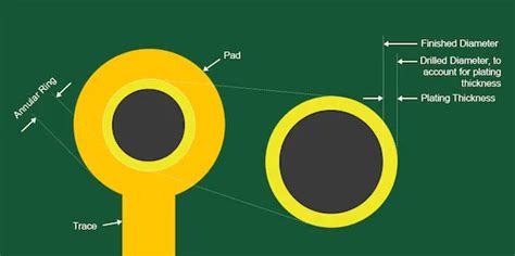
4. Copper Plating Thickness
The thickness of the copper plating inside the via affects the minimum via size. Thicker plating reduces the effective diameter of the via, requiring a larger initial drill size to achieve the desired finished diameter.
5. Current Carrying Capacity
The current carrying capacity of a via depends on its cross-sectional area. Larger vias can handle higher currents without overheating, while smaller vias are suitable for lower current applications.

Standard PCB Via Sizes
PCB via sizes are typically expressed in mils (thousandths of an inch) or millimeters. Some standard via sizes for different PCB thicknesses are:
| PCB Thickness (mm) | Minimum Via Diameter (mm) | Drill Size (mm) |
|---|---|---|
| 0.4 | 0.2 | 0.1 |
| 0.8 | 0.3 | 0.2 |
| 1.6 | 0.4 | 0.3 |
| 2.4 | 0.5 | 0.4 |
Note that these are general guidelines, and the actual minimum via size may vary depending on the PCB manufacturer’s capabilities and the specific design requirements.

Calculating PCB Via Size
To calculate the minimum via size for a given PCB thickness, use the following formula:
Minimum Via Diameter = (PCB Thickness / Aspect Ratio) + (2 × Copper Plating Thickness)
For example, for a 1.6mm thick PCB with an aspect ratio of 8:1 and a copper plating thickness of 25µm (0.025mm):
Minimum Via Diameter = (1.6mm / 8) + (2 × 0.025mm) = 0.25mm
In this case, the minimum via diameter would be 0.25mm, which is close to the 0.3mm drill size recommended in the table above.

Impact of Via Size on PCB Design
1. Board Size and Density
Smaller vias allow for denser PCB layouts, as they take up less space and can be placed closer together. This is particularly important for high-density designs, such as smartphones, wearables, and other compact electronic devices.
2. Signal Integrity
Via size can impact signal integrity, particularly at high frequencies. Smaller vias have lower capacitance and inductance, which can help minimize signal reflections and distortions. However, smaller vias also have higher resistance, which can lead to increased signal attenuation.
3. Manufacturing Cost
Smaller vias require more precise drilling and plating processes, which can increase manufacturing costs. Additionally, smaller drill bits are more expensive and prone to wear and breakage, further adding to production expenses.
Advanced Via Techniques
Several advanced via techniques can be used to optimize PCB designs:
1. Via-in-Pad
Via-in-pad is a technique where vias are placed directly on component pads, saving space and improving signal routing. This method requires careful control of the via filling and capping processes to ensure a flat, solderable surface.
2. Stacked Vias
Stacked vias are used to connect multiple layers in a PCB by placing vias on top of each other. This technique can save space and simplify routing but requires precise alignment and drilling to ensure proper connections.
3. Microvias
Microvias, as mentioned earlier, are small, laser-drilled vias used in HDI PCBs. They enable higher connection density and can be used to create stacked via structures for even greater space savings.
FAQ
1. What is the minimum via size for a 1.6mm thick PCB?
The minimum via size for a 1.6mm thick PCB depends on the aspect ratio and copper plating thickness. Assuming an aspect ratio of 8:1 and a copper plating thickness of 25µm, the minimum via diameter would be approximately 0.25mm, with a recommended drill size of 0.3mm.
2. Can I use smaller vias to save space on my PCB?
Yes, using smaller vias can help save space and increase component density on your PCB. However, smaller vias may also increase manufacturing costs and have an impact on signal integrity, particularly at high frequencies.
3. What is the difference between blind and buried vias?
Blind vias connect an outer layer to an inner layer without going through the entire PCB, while buried vias connect inner layers without reaching either the top or bottom layer of the board.
4. How does via size affect current carrying capacity?
The current carrying capacity of a via depends on its cross-sectional area. Larger vias can handle higher currents without overheating, while smaller vias are suitable for lower current applications.
5. What advanced via techniques can help optimize PCB designs?
Advanced via techniques such as via-in-pad, stacked vias, and microvias can help optimize PCB designs by saving space, improving signal routing, and increasing connection density. However, these techniques may require more precise manufacturing processes and increase production costs.
Conclusion
PCB via size is a critical aspect of PCB design, influencing factors such as board density, signal integrity, and manufacturing cost. Understanding the factors affecting via size, standard via sizes for different PCB thicknesses, and advanced via techniques can help designers create more efficient and reliable PCBs.
By carefully considering via size and utilizing appropriate design techniques, PCB designers can optimize their designs for specific applications, whether prioritizing space savings, signal integrity, or cost-effectiveness.
No responses yet