Introduction to PCB reflow Soldering
Reflow soldering is a process used in the manufacturing of printed circuit boards (PCBs) to attach surface mount components to the board. It involves applying solder paste to the PCB, placing the components, and then heating the entire assembly in a reflow oven to melt the solder and form a permanent connection. PCB reflow soldering is a crucial step in the production of electronic devices, as it ensures reliable and secure connections between components and the circuit board.
Advantages of Reflow Soldering
Reflow soldering offers several advantages over other soldering methods, such as wave soldering or hand soldering:
- Efficiency: Reflow soldering allows for the simultaneous soldering of multiple components, making it a highly efficient process for mass production.
- Consistency: The automated nature of reflow soldering ensures consistent and reliable solder joints across the entire PCB.
- Precision: Reflow soldering enables the use of smaller components and finer pitch sizes, allowing for more compact and complex PCB designs.
- Reduced thermal stress: The controlled heating and cooling cycles in reflow soldering minimize thermal stress on the components and the PCB.
The Reflow Soldering Process
The PCB reflow soldering process consists of several key steps:
1. Solder Paste Application
Solder paste, a mixture of tiny solder particles and flux, is applied to the PCB using a stencil or screen printing process. The stencil is a thin metal sheet with apertures that match the pads on the PCB. The solder paste is spread over the stencil, filling the apertures and depositing the paste onto the pads when the stencil is removed.
2. Component Placement
Surface mount components are placed onto the solder paste-covered pads using a pick-and-place machine. These machines use vacuum nozzles or grippers to pick up the components from feeders and accurately position them on the PCB. The adhesive properties of the solder paste help to hold the components in place during the subsequent reflow process.
3. Reflow Oven Processing
The PCB assembly is then passed through a reflow oven, which consists of several temperature-controlled zones. The oven heats the assembly according to a specific temperature profile, which typically includes the following stages:
- Preheat: The PCB is gradually heated to activate the flux and remove any moisture from the solder paste and components.
- Soak: The temperature is maintained for a specific duration to ensure even heat distribution and to allow the flux to clean the component leads and PCB pads.
- Reflow: The temperature is raised above the melting point of the solder, causing the solder particles to melt and form a connection between the components and the PCB pads.
- Cooling: The PCB is cooled at a controlled rate to allow the solder joints to solidify and prevent thermal shock to the components.
4. Inspection and Testing
After the reflow soldering process, the PCB undergoes visual inspection and electrical testing to ensure the quality and functionality of the solder joints and the overall assembly. Automated optical inspection (AOI) systems can be used to detect defects such as bridging, insufficient solder, or misaligned components. Electrical testing, such as in-circuit testing (ICT) or functional testing, verifies the electrical performance of the PCB.

Reflow Soldering Temperature Profile
The temperature profile is a critical aspect of the reflow soldering process, as it determines the quality and reliability of the solder joints. A well-designed temperature profile ensures that the solder melts and flows properly, while minimizing the risk of component damage or PCB Warpage.
A typical reflow soldering temperature profile consists of four main stages:
| Stage | Temperature Range | Duration |
|---|---|---|
| Preheat | 25°C to 150°C | 60-90 seconds |
| Soak | 150°C to 180°C | 60-120 seconds |
| Reflow | 220°C to 250°C | 30-60 seconds |
| Cooling | 250°C to 25°C | 60-120 seconds |
The specific temperatures and durations may vary depending on the type of solder paste, components, and PCB substrate used. It is essential to follow the recommended temperature profile provided by the solder paste manufacturer and to optimize the profile for the specific assembly.

Solder Paste Selection
Selecting the appropriate solder paste is crucial for achieving high-quality solder joints in PCB reflow soldering. Solder paste consists of solder alloy particles suspended in a flux medium. The main factors to consider when choosing a solder paste include:
- Alloy composition: The most common solder alloys used in reflow soldering are tin-lead (SnPb) and lead-free alloys, such as tin-silver-copper (SAC). Lead-free alloys have become more prevalent due to environmental and health concerns.
- Particle size: Solder paste is classified by the size of the solder particles, with Type 3 (25-45 microns) and Type 4 (20-38 microns) being the most commonly used in SMT assembly.
- Flux type: The flux in the solder paste helps to remove oxides and improve wetting during the soldering process. Fluxes are classified as rosin-based (RO), water-soluble (OA), or no-clean (NC), depending on their chemical composition and residue cleaning requirements.
- Viscosity and rheology: The solder paste’s viscosity and rheological properties affect its printability, slump resistance, and tack time, which are essential for maintaining component placement accuracy during the reflow process.

Stencil Design and Printing
Stencil design and printing play a critical role in depositing the correct amount of solder paste onto the PCB pads. A well-designed stencil ensures consistent solder paste volume and placement, which is essential for achieving reliable solder joints.
Stencil Design Considerations
- Aperture size and shape: The stencil apertures should be sized and shaped to match the PCB pads, taking into account the solder paste’s volume requirements and the component’s lead or termination design.
- Stencil thickness: The stencil thickness determines the solder paste volume deposited onto the pads. Typical stencil thicknesses range from 0.1 mm to 0.2 mm (4-8 mils), depending on the component size and pitch.
- Aperture wall tapering: Tapered aperture walls help to improve solder paste release and prevent clogging, especially for fine-pitch components.
- Fiducial marks: Fiducial marks on the stencil and PCB aid in aligning the stencil and ensuring accurate solder paste placement.
Stencil Printing Process
- Alignment: The stencil is aligned with the PCB using the fiducial marks and fixed in place on the printing machine.
- Solder paste application: Solder paste is dispensed onto the stencil and spread across the apertures using a squeegee blade.
- Printing: The squeegee blade is moved across the stencil, forcing the solder paste through the apertures and onto the PCB pads.
- Stencil removal: The stencil is carefully lifted from the PCB, leaving the solder paste deposits on the pads.
- Inspection: The printed PCB is inspected for solder paste quality, volume, and alignment, often using automated solder paste inspection (SPI) systems.
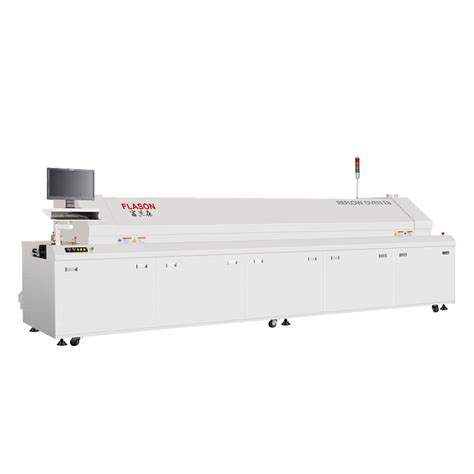
Reflow Oven Types and Features
Reflow ovens are essential equipment in the PCB reflow soldering process, providing the controlled heating and cooling necessary for forming reliable solder joints. There are several types of reflow ovens, each with specific features and benefits.
Convection Reflow Ovens
Convection reflow ovens are the most common type used in PCB assembly. They use forced air circulation to heat the PCB and components, providing a uniform and efficient heat transfer. Convection ovens can be further classified as:
- Horizontal convection ovens: PCBs are transported through the oven on a conveyor belt, passing through multiple heating zones.
- Vertical convection ovens: PCBs are placed vertically in a carrier and moved through the oven, allowing for better space utilization and reduced floor space requirements.
Infrared (IR) Reflow Ovens
Infrared reflow ovens use IR heating elements to heat the PCB and components directly. IR ovens offer faster heating rates and more precise temperature control compared to convection ovens. However, they may cause uneven heating due to the varying absorption rates of different materials and component shapes.
Vapor Phase Reflow Ovens
Vapor phase reflow ovens use a heated, inert fluid (typically a perfluoropolyether) to transfer heat to the PCB and components. The fluid evaporates, creating a vapor that condenses on the cooler PCB surface, providing a uniform and efficient heat transfer. Vapor phase reflow ovens offer excellent temperature stability and minimal temperature gradients, making them suitable for complex, high-density PCB assemblies.
Nitrogen Atmosphere Reflow Ovens
Nitrogen atmosphere reflow ovens use nitrogen gas to displace oxygen in the oven chamber, creating an inert environment during the soldering process. This reduces oxidation and improves solder joint quality, particularly for lead-free soldering processes that require higher temperatures and are more susceptible to oxidation.
Defects and Troubleshooting in PCB Reflow Soldering
Despite the automated nature of PCB reflow soldering, defects can still occur due to various factors such as improper solder paste application, component placement errors, or incorrect reflow temperature profiles. Common defects include:
- Bridging: Solder bridges form between adjacent pads or leads, causing short circuits.
- Insufficient solder: Inadequate solder volume results in weak or open connections.
- Tombstoning: Components stand up on one end due to uneven heating or pad design.
- Solder balls: Small solder spheres form on the PCB surface, potentially causing short circuits.
- Component shifting: Components move from their intended positions during the reflow process.
Troubleshooting and preventing these defects involves:
- Optimizing the solder paste printing process and stencil design.
- Ensuring accurate component placement and alignment.
- Adjusting the reflow temperature profile to suit the specific assembly requirements.
- Maintaining proper oven maintenance and calibration.
- Implementing robust inspection and quality control procedures.
Frequently Asked Questions (FAQ)
-
Q: What is the difference between reflow soldering and wave soldering?
A: Reflow soldering is used for surface mount components and involves applying solder paste, placing components, and heating the assembly in a reflow oven. Wave soldering is used for through-hole components and involves passing the PCB over a molten solder wave to form the solder joints. -
Q: Can reflow soldering be used for through-hole components?
A: While reflow soldering is primarily used for surface mount components, it can be used for certain through-hole components with appropriate adaptations, such as using solder paste in the through-holes or employing pin-in-paste techniques. -
Q: What is the purpose of nitrogen in reflow soldering?
A: Nitrogen is used in reflow soldering to create an inert atmosphere, reducing oxidation and improving solder joint quality. This is particularly important for lead-free soldering processes that require higher temperatures and are more prone to oxidation. -
Q: How do I select the right solder paste for my PCB assembly?
A: When selecting solder paste, consider factors such as the alloy composition (lead-free or tin-lead), particle size (Type 3 or Type 4), flux type (rosin-based, water-soluble, or no-clean), and rheological properties (viscosity and slump resistance). Consult with your solder paste supplier and consider your specific assembly requirements. -
Q: What are the key considerations for designing a reflow temperature profile?
A: When designing a reflow temperature profile, consider the solder paste activation temperature, soak time, peak temperature, and cooling rate. The profile should be optimized to ensure proper solder melting and wetting while minimizing thermal stress on the components and PCB. Follow the solder paste manufacturer’s recommendations and conduct profile validation tests to ensure the best results.
Conclusion
PCB reflow soldering is a critical process in the manufacturing of electronic devices, enabling the efficient and reliable attachment of surface mount components to printed circuit boards. By understanding the fundamentals of reflow soldering, including the process steps, temperature profile, solder paste selection, stencil design, and troubleshooting, engineers and technicians can optimize their PCB assembly processes and ensure high-quality solder joints.
As technology advances and miniaturization continues to drive the electronics industry, reflow soldering techniques and equipment will evolve to meet the challenges of increasingly complex and dense PCB designs. Staying up-to-date with the latest developments in materials, processes, and automation will be essential for maintaining a competitive edge in the fast-paced world of electronic manufacturing.
No responses yet