Introduction to SMT Stencils and Their Importance in PCB Assembly
Surface Mount Technology (SMT) has revolutionized the electronics industry by enabling the production of smaller, faster, and more efficient printed circuit boards (PCBs). One of the critical components in the SMT assembly process is the stencil, which is used to apply solder paste onto the PCB pads. The accuracy and precision of the stencil directly impact the quality of the solder joints and the overall reliability of the assembled PCB.
In this article, we will dive into the process of making holes in SMT stencils, exploring various techniques, best practices, and troubleshooting tips to ensure optimal stencil performance.
Understanding SMT Stencil Materials and Thicknesses
Before delving into the hole-making process, it’s essential to understand the different materials and thicknesses used for SMT stencils.
Stencil Materials
SMT stencils are typically made from one of the following materials:
- Stainless Steel
- Nickel
- Polyimide (Kapton)
- Mylar
Each material has its advantages and disadvantages, as summarized in the table below:
| Material | Advantages | Disadvantages |
|---|---|---|
| Stainless Steel | Durable, long lifespan, suitable for high-volume production | Expensive, prone to warping, requires frequent cleaning |
| Nickel | Good durability, less prone to warping than stainless steel | Expensive, requires frequent cleaning |
| Polyimide (Kapton) | Lightweight, flexible, cost-effective | Limited lifespan, not suitable for high-volume production |
| Mylar | Lightweight, flexible, cost-effective | Limited lifespan, not suitable for high-volume production |
Stencil Thicknesses
The thickness of an SMT stencil is critical in determining the amount of solder paste deposited onto the PCB pads. Common stencil thicknesses range from 0.1 mm to 0.2 mm (4 to 8 mils), with the most popular being:
- 0.1 mm (4 mils)
- 0.12 mm (5 mils)
- 0.15 mm (6 mils)
The choice of stencil thickness depends on factors such as component size, pad geometry, and solder paste rheology.

Techniques for Making Holes in SMT Stencils
There are several methods for creating holes in SMT stencils, each with its own advantages and limitations. The most common techniques include:
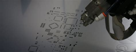
Laser Cutting
Laser cutting is a precise and efficient method for creating holes in SMT stencils. It involves using a high-powered laser to vaporize the stencil material, resulting in clean and accurate apertures. Laser cutting is suitable for both metal and polymer stencils and can handle complex geometries and fine pitches.
Advantages:
– High precision and accuracy
– Fast and efficient process
– Suitable for complex geometries and fine pitches
Disadvantages:
– Expensive equipment
– Requires skilled operators
– May cause heat-affected zones in metal stencils
Chemical Etching
Chemical etching is a subtractive process that uses a chemical solution to remove material from the stencil surface. The stencil is first coated with a photoresist, which is then exposed to UV light through a photomask containing the desired aperture pattern. The exposed areas of the photoresist are dissolved, allowing the chemical solution to etch away the underlying stencil material.
Advantages:
– Cost-effective for large-volume production
– Suitable for fine pitches and complex geometries
– Minimal heat-affected zones in metal stencils
Disadvantages:
– Slower process compared to laser cutting
– Requires careful control of etching parameters
– Generates chemical waste that needs proper disposal
Electroforming
Electroforming is an additive process that involves growing a metal layer (usually nickel) onto a conductive mandrel or master. The mandrel is first created with the desired aperture pattern using photolithography or CNC machining. The mandrel is then placed in an electroplating bath, where nickel ions are deposited onto the surface, forming a thin metal layer that replicates the aperture pattern.
Advantages:
– Produces high-quality stencils with smooth aperture walls
– Suitable for fine pitches and complex geometries
– Minimal heat-affected zones
Disadvantages:
– Slow and expensive process
– Limited to metal stencils (usually nickel)
– Requires specialized equipment and skilled operators

Best Practices for Making Holes in SMT Stencils
To ensure optimal stencil performance and solder paste deposition, consider the following best practices when making holes in SMT stencils:
-
Aperture Design: Ensure that the aperture dimensions and shape are optimized for the specific component and pad geometry. Consider factors such as aspect ratio, area ratio, and solder paste release characteristics.
-
Aperture Placement: Maintain sufficient spacing between apertures to prevent solder paste bridging and ensure proper gasketing during printing. Follow the manufacturer’s guidelines for minimum aperture spacing and stencil thickness.
-
Stencil Thickness: Select the appropriate stencil thickness based on the component size, pad geometry, and solder paste rheology. Thinner stencils are suitable for smaller components and fine-pitch applications, while thicker stencils are better for larger components and higher solder paste volumes.
-
Aperture Wall Quality: Ensure that the aperture walls are smooth and free from burrs, roughness, or tapering. Poor aperture wall quality can lead to inconsistent solder paste release and compromised print quality.
-
Stencil Cleaning and Maintenance: Regularly clean the stencil using appropriate solvents and methods to prevent solder paste buildup and contamination. Proper maintenance extends the stencil lifespan and ensures consistent print quality.

Troubleshooting Common Issues in SMT Stencil Hole Making
Despite following best practices, issues may arise during the stencil hole-making process. Some common problems and their potential solutions include:
-
Overetching or Underetching (Chemical Etching): Adjust the etching time, temperature, or chemical concentration to achieve the desired aperture dimensions. Conduct test etches on sample stencils to optimize the process parameters.
-
Heat-Affected Zones (Laser Cutting): Optimize the laser power, speed, and focal point to minimize heat-affected zones in metal stencils. Consider using pulsed lasers or special coatings to reduce thermal damage.
-
Poor Aperture Wall Quality: Ensure proper process control during laser cutting, chemical etching, or electroforming. Regularly inspect the aperture walls using microscopy and address any issues with the process parameters or equipment maintenance.
-
Stencil Warping or Distortion: Maintain proper tension and support during the hole-making process to prevent stencil warping or distortion. Use specialized frames or fixtures to hold the stencil flat and stable.
-
Inconsistent Aperture Dimensions: Regularly calibrate and maintain the hole-making equipment to ensure consistent aperture dimensions across the stencil. Implement quality control measures, such as optical inspection or 3D profiling, to verify the aperture dimensions and shape.
Frequently Asked Questions (FAQs)
-
What is the most suitable stencil material for high-volume production?
Stainless steel and nickel stencils are the most suitable materials for high-volume production due to their durability and long lifespan. However, they are more expensive and require frequent cleaning compared to polymer stencils. -
How do I select the appropriate stencil thickness for my application?
The choice of stencil thickness depends on factors such as component size, pad geometry, and solder paste rheology. As a general guideline, use thinner stencils (0.1-0.12 mm) for smaller components and fine-pitch applications, and thicker stencils (0.15-0.2 mm) for larger components and higher solder paste volumes. Consult with your stencil manufacturer or solder paste supplier for specific recommendations. -
What is the difference between laser cutting and chemical etching for making holes in SMT stencils?
Laser cutting is a fast and precise method that uses a high-powered laser to vaporize the stencil material, while chemical etching is a slower process that uses a chemical solution to remove material from the stencil surface. Laser cutting is suitable for both metal and polymer stencils and can handle complex geometries and fine pitches, but it requires expensive equipment and skilled operators. Chemical etching is more cost-effective for large-volume production but generates chemical waste that needs proper disposal. -
How often should I clean my SMT stencil, and what cleaning methods are recommended?
The frequency of stencil cleaning depends on factors such as the solder paste type, printing volume, and environment. As a general guideline, clean the stencil every 4-8 hours of continuous printing or when print quality issues arise. Use appropriate solvents (such as isopropyl alcohol) and cleaning methods (such as manual wiping, ultrasonic cleaning, or automated stencil cleaners) as recommended by the stencil manufacturer or solder paste supplier. -
What are the consequences of poor aperture wall quality in SMT stencils?
Poor aperture wall quality, such as roughness, burrs, or tapering, can lead to inconsistent solder paste release and compromised print quality. This can result in insufficient or excessive solder paste deposition, solder bridges, or poor solder joint formation, ultimately affecting the reliability and performance of the assembled PCB. Ensuring smooth and high-quality aperture walls is crucial for optimal stencil performance.
Conclusion
Making holes in SMT stencils is a critical aspect of the PCB assembly process, directly impacting the quality and reliability of the solder joints. By understanding the different stencil materials, thicknesses, and hole-making techniques, manufacturers can optimize their stencil design and production for specific applications.
Implementing best practices, such as proper aperture design, placement, and maintenance, can help ensure consistent and high-quality solder paste deposition. Regularly troubleshooting and addressing common issues in the hole-making process is essential for maintaining optimal stencil performance and minimizing production delays or quality issues.
As technology advances and component sizes continue to shrink, the importance of precise and reliable SMT stencils will only grow. Staying up-to-date with the latest developments in stencil materials, hole-making techniques, and best practices will be crucial for manufacturers to remain competitive and meet the evolving demands of the electronics industry.
No responses yet