What is the LM358 op-amp?
The LM358 is a dual low-power operational amplifier with two independent, high-gain amplifiers in a single package. It is designed for a wide range of analog applications, such as signal conditioning, active filtering, and voltage comparisons. The IC is manufactured by several companies, including Texas Instruments, ON Semiconductor, and STMicroelectronics.
Key features of the LM358
- Dual op-amp in a single package
- Low supply current drain (500 µA/amplifier)
- Wide supply voltage range (3V to 32V for LM358, 3V to 16V for LM358A)
- Input common-mode voltage range includes ground
- Differential input voltage range equal to the power supply voltage
- Large DC voltage gain (100 dB)
- Wide bandwidth (1 MHz)
- Low input bias current (45 nA)
- Low input offset voltage (2 mV) and offset current (5 nA)
- Output short-circuit protection
- No latch-up when input common-mode range is exceeded
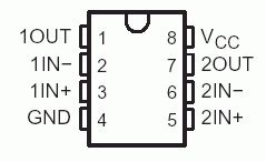
LM358 Pinout and Package
The LM358 is available in several package types, including 8-pin DIP (Dual Inline Package), 8-pin SOIC (Small Outline Integrated Circuit), and 8-pin TSSOP (Thin Shrink Small Outline Package). The pinout for the LM358 is as follows:
| Pin | Function |
|---|---|
| 1 | Output A |
| 2 | Inverting Input A |
| 3 | Non-Inverting Input A |
| 4 | Ground |
| 5 | Non-Inverting Input B |
| 6 | Inverting Input B |
| 7 | Output B |
| 8 | V+ (Positive Supply) |

LM358 Specifications
Absolute Maximum Ratings
| Parameter | Value |
|---|---|
| Supply Voltage (V+) | 32V (LM358), 16V (LM358A) |
| Input Differential Voltage | 32V (LM358), 16V (LM358A) |
| Input Common-Mode Voltage | -0.3V to V+ + 0.3V |
| Output Short-Circuit Duration | Indefinite |
| Operating Temperature Range | 0°C to +70°C |
| Storage Temperature Range | -65°C to +150°C |
Electrical Characteristics
| Parameter | Conditions | Min | Typ | Max | Unit |
|---|---|---|---|---|---|
| Input Offset Voltage | TA = 25°C | – | 2 | 7 | mV |
| Input Bias Current | TA = 25°C | – | 45 | 250 | nA |
| Input Offset Current | TA = 25°C | – | 5 | 50 | nA |
| Large Signal Voltage Gain | RL ≥ 2 kΩ, TA = 25°C | 50 | 100 | – | V/mV |
| Output Voltage Swing | RL ≥ 10 kΩ, TA = 25°C | 0 | – | V+ – 1.5 | V |
| Supply Current (per amplifier) | TA = 25°C | – | 0.5 | 1.2 | mA |
| Slew Rate | TA = 25°C | – | 0.6 | – | V/µs |
| Gain-Bandwidth Product | TA = 25°C | – | 1 | – | MHz |
| Input Voltage Range | TA = 25°C | 0 | – | V+ – 1.5 | V |
| Common-Mode Rejection Ratio | TA = 25°C | – | 70 | – | dB |
| Power Supply Rejection Ratio | TA = 25°C | – | 65 | – | dB |

LM358 Applications
The LM358 is suitable for a wide range of analog applications, including:
- Signal conditioning
- Amplification
- Buffering
- Filtering
-
Level shifting
-
Active filters
- Low-pass filters
- High-pass filters
- Band-pass filters
-
Notch filters
- Window comparators
- Schmitt triggers
-
Level detectors
-
Instrumentation
- Sensor amplification (e.g., thermocouples, strain gauges)
- Current sensing
-
Transducer interfacing
-
Audio applications
- Preamplifiers
- Tone controls
- Mixers
-
Equalizers
-
Power supply regulation
- Adjustable voltage regulators
- Current limiters
-
Overvoltage protection
-
Waveform generation
- Square wave generators
- Triangle wave generators
-
Sawtooth wave generators
-
Analog computation
- Summing amplifiers
- Difference amplifiers
- Integrators
- Differentiators

Basic LM358 Circuits
Inverting Amplifier
An inverting amplifier using the LM358 can be designed using the following formula:
Vout = -(Rf / Rin) * Vin
Where:
– Vout is the output voltage
– Vin is the input voltage
– Rf is the feedback resistor
– Rin is the input resistor
Non-Inverting Amplifier
A non-inverting amplifier using the LM358 can be designed using the following formula:
Vout = (1 + Rf / R1) * Vin
Where:
– Vout is the output voltage
– Vin is the input voltage
– Rf is the feedback resistor
– R1 is the resistor between the inverting input and ground
Voltage Comparator
A voltage comparator using the LM358 can be designed by connecting the reference voltage to the non-inverting input and the signal to be compared to the inverting input. The output will be high when the signal is lower than the reference voltage and low when the signal is higher than the reference voltage.
LM358 Usage Tips
-
Decoupling capacitors: Use 0.1 µF ceramic capacitors between the positive supply (V+) and ground, as close to the IC as possible, to reduce noise and ensure stable operation.
-
Input voltage range: Ensure that the input voltage remains within the specified common-mode and differential voltage ranges to avoid distortion or damage to the IC.
-
Output current: The LM358 can sink or source up to 20 mA of output current. If higher current is required, use a buffer stage or a more powerful op-amp.
-
Gain-bandwidth product: Consider the gain-bandwidth product when designing high-frequency applications. The LM358 has a gain-bandwidth product of 1 MHz, which limits the maximum achievable bandwidth for a given gain.
-
Offset voltage: In applications sensitive to offset voltage, consider using external offset nulling techniques or a more precise op-amp.
-
PCB layout: Ensure proper PCB layout techniques, such as minimizing trace lengths, separating analog and digital grounds, and using ground planes to reduce noise and interference.
Frequently Asked Questions (FAQ)
-
Q: Can the LM358 be used with a single supply?
A: Yes, the LM358 can operate with a single supply voltage as low as 3V. The input common-mode voltage range includes ground, allowing for single-supply operation. -
Q: What is the maximum supply voltage for the LM358?
A: The maximum supply voltage for the LM358 is 32V, while the LM358A has a maximum supply voltage of 16V. Always refer to the datasheet for the specific version of the IC you are using. -
Q: Is the LM358 suitable for audio applications?
A: Yes, the LM358 can be used in various audio applications, such as preamplifiers, tone controls, and mixers. However, for high-fidelity audio applications, op-amps with lower noise and distortion characteristics may be more suitable. -
Q: Can the LM358 be used as a comparator?
A: Yes, the LM358 can be used as a voltage comparator. Connect the reference voltage to the non-inverting input and the signal to be compared to the inverting input. The output will switch between high and low based on the relative levels of the two inputs. -
Q: How can I reduce the offset voltage of the LM358?
A: To reduce the offset voltage of the LM358, you can use external offset nulling techniques, such as adding a potentiometer between the offset null pins (if available) or using a voltage divider at the non-inverting input. Alternatively, you can use a more precise op-amp with lower offset voltage specifications.
Conclusion
The LM358 is a versatile and cost-effective dual op-amp that finds applications in a wide range of analog circuits. Its key features, such as low power consumption, wide supply voltage range, and input common-mode voltage range including ground, make it a popular choice for many designers. By understanding the LM358’s specifications, applications, and usage tips, you can effectively incorporate this op-amp into your designs and create robust, efficient analog circuits.
No responses yet