What is Back Drill PCB?
Back drill PCB, also known as controlled depth drilling or back-drilling, is a technique used in the manufacturing of printed circuit boards (PCBs) to improve signal integrity and reduce signal reflections. In high-speed digital circuits, signal reflections can occur when there is an impedance mismatch between the signal trace and the via stub. Back drilling involves removing the unwanted portion of the via stub, which reduces the capacitance and inductance of the via, thereby improving signal integrity.
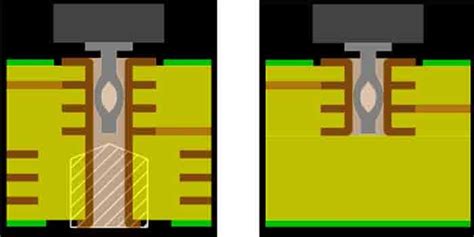
How Back Drilling Works
Back drilling is performed after the PCB has been fabricated and plated. The process involves drilling a larger diameter hole concentric with the original via hole, but only partially through the board, leaving a short stub at the signal layer. The depth of the back drill is carefully controlled to remove the unwanted portion of the via stub while leaving enough of the via to maintain the electrical connection.
The back drilling process typically follows these steps:
- The PCB is placed on a specialized back drilling machine.
- The machine uses a larger diameter drill bit to create a concentric hole partially through the board, removing the unwanted portion of the via stub.
- The depth of the back drill is carefully controlled to ensure that the electrical connection is maintained.
- The process is repeated for all the vias that require back drilling.
Benefits of Back Drilling
Back drilling offers several benefits for high-speed digital circuits:
- Improved Signal Integrity: By reducing the capacitance and inductance of the via stub, back drilling minimizes signal reflections and improves signal integrity.
- Reduced EMI: Signal reflections can cause electromagnetic interference (EMI). By reducing signal reflections, back drilling can help reduce EMI.
- Higher Data Rates: With improved signal integrity, back drilling enables PCBs to support higher data rates and faster rise times.
- Increased Reliability: By reducing signal reflections and EMI, back drilling can improve the overall reliability of the PCB.
When to Use Back Drilling
Back drilling is typically used in high-speed digital circuits where signal integrity is critical. Some common applications include:
- High-Speed Digital Interfaces: Back drilling is often used in PCBs that support high-speed digital interfaces such as USB, PCIe, SATA, and HDMI.
- High-Frequency RF Circuits: Back drilling can be used in high-frequency RF circuits to improve signal integrity and reduce EMI.
- Multilayer PCBs: Back drilling is particularly useful in multilayer PCBs where signal traces must transition between layers using vias.

Designing for Back Drilling
When designing a PCB for back drilling, there are several factors to consider:
- Via Size: The size of the via and the back drill hole must be carefully selected to ensure that the electrical connection is maintained while removing the unwanted portion of the via stub.
- Via Placement: Vias should be placed strategically to minimize the number of vias that require back drilling.
- Signal Trace Routing: Signal traces should be routed to minimize the number of layer transitions and the length of the via stubs.
- Impedance Matching: The impedance of the signal traces and the vias should be carefully matched to minimize signal reflections.
Back Drilling Design Guidelines
Here are some general guidelines for designing PCBs for back drilling:
- Use the smallest via size possible to minimize the capacitance and inductance of the via.
- Place vias strategically to minimize the number of vias that require back drilling.
- Route signal traces to minimize the number of layer transitions and the length of the via stubs.
- Use impedance matching techniques to ensure that the impedance of the signal traces and the vias are well-matched.
- Specify the back drilling requirements clearly in the PCB fabrication drawing, including the via size, back drill depth, and any special requirements.
| Parameter | Recommended Value |
|---|---|
| Via Diameter | 0.2 mm – 0.5 mm |
| Back Drill Depth | 0.2 mm – 0.4 mm from the signal layer |
| Via Stub Length | Less than 0.5 mm |
| Impedance Matching | ± 10% of the target impedance |

Back Drilling Manufacturing Process
The back drilling manufacturing process requires specialized equipment and expertise. Here are the key steps involved in the back drilling process:
- PCB Fabrication: The PCB is fabricated using standard PCB manufacturing processes, including drilling, plating, and etching.
- Back Drilling Preparation: The PCB is loaded onto a specialized back drilling machine, and the back drilling parameters are programmed into the machine.
- Back Drilling: The machine uses a larger diameter drill bit to create a concentric hole partially through the board, removing the unwanted portion of the via stub. The depth of the back drill is carefully controlled to ensure that the electrical connection is maintained.
- Cleaning: After back drilling, the PCB is cleaned to remove any debris or burrs created during the drilling process.
- Inspection: The PCB is inspected to ensure that the back drilling process was performed correctly and that the electrical connections are intact.
Back Drilling Equipment
Back drilling requires specialized equipment that can precisely control the depth and position of the back drill hole. Some common types of back drilling equipment include:
- CNC Back Drilling Machines: These machines use computer numerical control (CNC) to precisely control the position and depth of the back drill hole.
- Laser Back Drilling Machines: These machines use a laser to remove the unwanted portion of the via stub, providing a high degree of precision and control.
- Plasma Back Drilling Machines: These machines use a plasma arc to remove the unwanted portion of the via stub, providing a fast and efficient back drilling process.
Back Drilling Quality Control
Quality control is critical in the back drilling process to ensure that the electrical connections are maintained and that the signal integrity is not compromised. Here are some common quality control measures used in the back drilling process:
- Visual Inspection: The PCB is visually inspected to ensure that the back drilling process was performed correctly and that there are no visible defects or damage.
- Electrical Testing: The PCB is electrically tested to ensure that the electrical connections are intact and that the signal integrity is not compromised.
- Cross-Sectional Analysis: A cross-sectional analysis of the back drilled via can be performed to verify that the back drill depth and profile are within specifications.
- Time-Domain Reflectometry (TDR): TDR can be used to measure the impedance of the via and to detect any signal reflections caused by the via stub.

Advantages and Disadvantages of Back Drilling
Like any manufacturing process, back drilling has its advantages and disadvantages. Here are some of the key advantages and disadvantages of back drilling:
Advantages
- Improved Signal Integrity: Back drilling can significantly improve signal integrity by reducing the capacitance and inductance of the via stub, minimizing signal reflections.
- Reduced EMI: By reducing signal reflections, back drilling can help reduce electromagnetic interference (EMI).
- Higher Data Rates: With improved signal integrity, back drilling enables PCBs to support higher data rates and faster rise times.
- Increased Reliability: By reducing signal reflections and EMI, back drilling can improve the overall reliability of the PCB.
Disadvantages
- Increased Cost: Back drilling adds an additional step to the PCB manufacturing process, which can increase the overall cost of the PCB.
- Limited Availability: Not all PCB manufacturers offer back drilling services, which can limit the availability of back drilled PCBs.
- Longer Lead Times: Back drilling can add additional time to the PCB manufacturing process, which can increase lead times.
- Limited Via Size: Back drilling is typically limited to larger via sizes, which can limit the design flexibility of the PCB.
Conclusion
Back drilling is a powerful technique for improving signal integrity and reducing signal reflections in high-speed digital circuits. By removing the unwanted portion of the via stub, back drilling can reduce the capacitance and inductance of the via, enabling PCBs to support higher data rates and faster rise times. When designing PCBs for back drilling, it is important to carefully consider the via size, placement, and signal trace routing to ensure that the electrical connections are maintained and that the signal integrity is not compromised. While back drilling does add additional cost and complexity to the PCB manufacturing process, the benefits of improved signal integrity and reduced EMI make it a valuable tool for high-speed digital designs.
Frequently Asked Questions (FAQ)
-
What is back drilling in PCB manufacturing?
Back drilling is a technique used in PCB manufacturing to remove the unwanted portion of the via stub, reducing the capacitance and inductance of the via and improving signal integrity. -
When is back drilling typically used?
Back drilling is typically used in high-speed digital circuits where signal integrity is critical, such as USB, PCIe, SATA, and HDMI interfaces, as well as in high-frequency RF circuits and multilayer PCBs. -
What are the benefits of back drilling?
The benefits of back drilling include improved signal integrity, reduced EMI, higher data rates, and increased reliability. -
What are the disadvantages of back drilling?
The disadvantages of back drilling include increased cost, limited availability, longer lead times, and limited via size. -
What factors should be considered when designing PCBs for back drilling?
When designing PCBs for back drilling, factors such as via size, via placement, signal trace routing, and impedance matching should be carefully considered to ensure that the electrical connections are maintained and that the signal integrity is not compromised.
No responses yet