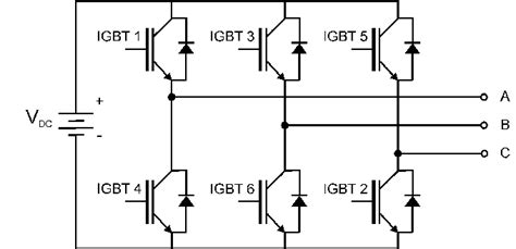
Introduction to IGBT
An Insulated Gate Bipolar Transistor (IGBT) is a power semiconductor device that combines the best features of both MOSFETs and bipolar junction transistors (BJTs). It has become a popular choice for high-power applications due to its superior performance characteristics, such as high current density, low on-state voltage drop, and fast switching speeds.
What is an IGBT?
An IGBT is a three-terminal device that consists of a gate, collector, and emitter. The gate is insulated from the collector-emitter channel by a thin oxide layer, similar to a MOSFET. The collector-emitter channel, however, is made up of a p-type substrate with an n-type epitaxial layer, which allows for conductivity modulation and higher current densities compared to a MOSFET.
Advantages of IGBTs
- High current density
- Low on-state voltage drop
- Fast switching speeds
- Easy to control with a low-power gate signal
- Rugged and reliable
IGBT Structure
Basic Structure
An IGBT consists of four layers: a p+ substrate, an n- drift region, a p-well, and an n+ emitter. The gate is insulated from the semiconductor layers by a thin oxide layer.
| Layer | Function |
|---|---|
| p+ substrate | Provides mechanical support and serves as the collector |
| n- drift region | Supports high blocking voltage and allows for conductivity modulation |
| p-well | Creates the channel for current flow when the device is turned on |
| n+ emitter | Provides a source of electrons for the channel and serves as the emitter |
Equivalent Circuit
The equivalent circuit of an IGBT can be represented as a combination of a MOSFET and a BJT. The MOSFET controls the current flow through the device, while the BJT provides conductivity modulation in the drift region, allowing for higher current densities.
IGBT Operation
On-State
When a positive voltage is applied to the gate, an inversion layer (channel) is formed in the p-well, allowing electrons to flow from the emitter to the collector. As the electrons move through the n- drift region, they attract holes from the p+ substrate, resulting in conductivity modulation and a low on-state voltage drop.
Off-State
When the gate voltage is removed or a negative voltage is applied, the channel disappears, and the device turns off. The n- drift region supports the high blocking voltage in the off-state.
Switching Characteristics
IGBTs have fast switching speeds, typically in the range of tens to hundreds of nanoseconds. The switching speed is limited by the time required to establish and remove the conductivity modulation in the drift region.

IGBT Applications
IGBTs are widely used in high-power applications, such as:
- Motor drives
- Power inverters
- Uninterruptible power supplies (UPS)
- Welding equipment
- Electric vehicles
- Renewable energy systems
IGBT Selection Considerations
When selecting an IGBT for a specific application, several factors should be considered:
- Voltage and current ratings
- Switching frequency
- Power dissipation
- Package type
- Cost
IGBT Protection and Reliability
To ensure reliable operation and prevent device failure, IGBTs require proper protection measures:
- Overcurrent protection
- Overvoltage protection
- Overtemperature protection
- Short-circuit protection
- Gate-drive circuit protection
Proper thermal management is also essential to maintain device reliability and prevent thermal runaway.
IGBT Advancements and Future Trends
Recent advancements in IGBT technology include:
- Trench-gate structures for improved performance
- Thin-wafer technology for reduced on-state voltage drop
- Silicon carbide (SiC) IGBTs for higher voltage and temperature operation
- Integration of protection and control functions into IGBT modules
Future trends in IGBT development include further improvements in performance, reliability, and cost reduction, as well as the adoption of wide-bandgap materials like SiC and gallium nitride (GaN) for even higher power densities and switching speeds.
Frequently Asked Questions (FAQ)
1. What is the difference between an IGBT and a MOSFET?
IGBTs have a higher current density and lower on-state voltage drop compared to MOSFETs due to conductivity modulation in the drift region. MOSFETs, on the other hand, have faster switching speeds and are better suited for lower power applications.
2. Can IGBTs be used in parallel?
Yes, IGBTs can be connected in parallel to increase the current handling capability. However, proper current sharing measures must be implemented to ensure equal distribution of current among the devices.
3. What is the maximum operating temperature of an IGBT?
The maximum operating temperature of an IGBT depends on the specific device and its packaging. Typically, silicon-based IGBTs have a maximum junction temperature of 150°C to 175°C, while SiC IGBTs can operate at temperatures up to 200°C or higher.
4. How do I select the appropriate IGBT for my application?
When selecting an IGBT, consider the voltage and current ratings, switching frequency, power dissipation, package type, and cost. Consult the manufacturer’s datasheets and application notes for guidance on device selection and design considerations.
5. What are the failure modes of IGBTs?
Common failure modes of IGBTs include overcurrent, overvoltage, overtemperature, and short-circuit conditions. Proper protection measures and thermal management are essential to prevent device failure and ensure reliable operation.
Conclusion
IGBTs have become a critical component in many high-power applications due to their superior performance characteristics and ease of control. By understanding the working principle, structure, operation, and applications of IGBTs, engineers can effectively design and implement power electronic systems that meet the demands of modern industry.
As IGBT technology continues to advance, with improvements in performance, reliability, and the adoption of wide-bandgap materials, we can expect to see even more innovative and efficient power electronic solutions in the future.

No responses yet