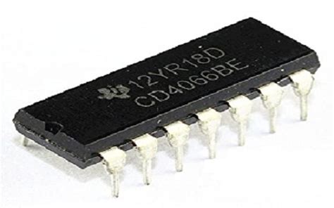
Introduction to CD4066
The CD4066 is a member of the 4000 series of CMOS (Complementary Metal-Oxide-Semiconductor) logic ICs. It consists of four independent bilateral switches, each capable of conducting signals in both directions when turned on. The IC is widely used in analog and digital signal routing, multiplexing, and various control applications.
Key Features of CD4066
- Quad bilateral switch package
- Low ON resistance (typically around 100Ω)
- High OFF resistance (>10^12 Ω)
- Wide supply voltage range (3V to 15V)
- Low power consumption
- High switching speed
- TTL and CMOS compatible logic levels
- Latch-up free operation
These features make the CD4066 an attractive choice for designers seeking a reliable and efficient switching solution.
Working Principle of CD4066
The CD4066 operates as a voltage-controlled switch, allowing or blocking the flow of signals based on the control voltage applied to its control pin. Each of the four switches in the IC has three terminals: IN/OUT, OUT/IN, and CONTROL.
Switch Operation
When the control voltage is low (typically below 1/3 of the supply voltage), the switch is turned off, and the IN/OUT and OUT/IN terminals are effectively disconnected. In this state, the switch exhibits a high resistance, preventing signal flow.
On the other hand, when the control voltage is high (typically above 2/3 of the supply voltage), the switch is turned on, and the IN/OUT and OUT/IN terminals are connected. The switch acts as a low-resistance path, allowing signals to pass through.
Signal Handling
One of the key advantages of the CD4066 is its ability to handle both analog and digital signals. The bilateral nature of the switches allows signals to flow in either direction when the switch is on. This feature enables the CD4066 to be used in a wide range of applications, from analog signal routing to digital multiplexing.
Switch Characteristics
The ON resistance of the CD4066 switches is typically around 100Ω, ensuring minimal signal attenuation when the switch is conducting. The OFF resistance is extremely high, typically exceeding 10^12 Ω, providing excellent isolation between the IN/OUT and OUT/IN terminals when the switch is off.
The switching speed of the CD4066 is relatively high, with typical transition times in the order of nanoseconds. This allows for fast signal routing and multiplexing applications.

Applications of CD4066
The CD4066 finds use in a multitude of electronic applications across various domains. Let’s explore some of the common applications of this versatile IC.
Analog Signal Switching
One of the primary applications of the CD4066 is in analog signal switching. The bilateral switches can be used to route analog signals between different stages of a circuit or to select between multiple analog sources. This is particularly useful in audio and video systems, where signals need to be routed to different processing blocks or outputs.
Analog Multiplexing
The CD4066 can be used to implement analog multiplexers, allowing the selection of one analog signal from multiple input signals. By cascading multiple CD4066 ICs, larger multiplexers can be constructed. This finds applications in data acquisition systems, where multiple analog sensors need to be monitored using a single analog-to-digital converter (ADC).
Sample and Hold Circuits
In sample and hold circuits, the CD4066 can be used as the switching element to capture and hold an analog voltage level. When the switch is turned on, the input signal is sampled and stored on a capacitor. When the switch is turned off, the capacitor holds the sampled voltage, allowing for further processing or conversion.
Digital Signal Multiplexing
The CD4066 can also be employed in digital signal multiplexing applications. By using the switches to select between multiple digital input signals, a multiplexed output can be generated. This is useful in digital communication systems, where multiple data streams need to be combined or selected.
Logic Level Shifting
In certain scenarios, the CD4066 can be used for logic level shifting between different voltage domains. By connecting the appropriate supply voltages to the IC and controlling the switches, signals can be translated from one logic level to another. This is handy when interfacing between different logic families or when dealing with varying supply voltages.
Chopper Stabilized Amplifiers
Chopper stabilized amplifiers are used to reduce low-frequency noise and offset voltage in precision analog circuits. The CD4066 can be used as the chopping switch, periodically swapping the input and output of the amplifier. This technique effectively modulates the input signal and removes the low-frequency noise components, resulting in improved signal-to-noise ratio and stability.
Audio and Video Switching
In audio and video systems, the CD4066 can be utilized for signal routing and switching. The low ON resistance and high OFF resistance of the switches ensure minimal signal degradation and crosstalk. This allows for seamless switching between different audio or video sources, such as selecting between multiple input channels or routing signals to different output devices.
Capacitance Multipliers
The CD4066 can be used to implement capacitance multipliers, which are circuits that effectively increase the capacitance of a given capacitor. By periodically switching the capacitor in and out of the circuit using the CD4066, the apparent capacitance seen by the circuit can be multiplied. This technique is useful in low-frequency filter designs and in applications where large capacitance values are required.

Frequently Asked Questions (FAQ)
1. What is the maximum supply voltage that can be applied to the CD4066?
The CD4066 can operate with a wide supply voltage range, typically from 3V to 15V. However, it is essential to consult the datasheet for the specific version of the CD4066 being used to ensure proper operation and to avoid exceeding the maximum ratings.
2. Can the CD4066 switches be used to control high-current loads?
No, the CD4066 switches are designed for signal switching and multiplexing applications. They are not intended to directly control high-current loads. If high-current switching is required, additional driver circuits or relay modules should be used in conjunction with the CD4066.
3. What is the maximum switching frequency of the CD4066?
The maximum switching frequency of the CD4066 depends on several factors, including the supply voltage, load capacitance, and the specific version of the IC. Typically, the CD4066 can operate at switching frequencies up to several megahertz (MHz). However, for accurate information, it is recommended to refer to the datasheet of the specific CD4066 variant being used.
4. How can multiple CD4066 ICs be cascaded to create larger multiplexers?
To create larger multiplexers using multiple CD4066 ICs, the switches can be connected in a tree-like structure. The control inputs of the switches are connected to the appropriate control signals, and the IN/OUT and OUT/IN terminals are connected to form the desired multiplexing configuration. By carefully designing the control logic and signal routing, multiplexers with a higher number of inputs can be realized.
5. Are there any precautions to be taken when handling the CD4066?
Yes, like most CMOS devices, the CD4066 is sensitive to electrostatic discharge (ESD). Proper ESD handling procedures should be followed when working with the IC to prevent damage. This includes using grounded wrist straps, anti-static mats, and handling the IC by its package rather than the pins. Additionally, the IC should be stored in anti-statIC Packaging when not in use.

Conclusion
The CD4066 is a highly versatile quad bilateral switch IC that finds extensive use in various analog and digital applications. Its key features, such as low ON resistance, high OFF resistance, wide supply voltage range, and the ability to handle both analog and digital signals, make it a popular choice among electronic designers.
Understanding the working principle of the CD4066 and its switch characteristics is crucial for effectively utilizing this IC in different applications. From analog signal switching and multiplexing to digital signal routing and logic level shifting, the CD4066 offers a wide range of possibilities.
By exploring the various applications of the CD4066, including sample and hold circuits, chopper stabilized amplifiers, audio and video switching, and capacitance multipliers, designers can leverage the capabilities of this IC to create efficient and reliable electronic systems.
As with any electronic component, proper handling and adherence to datasheet specifications are essential to ensure optimal performance and longevity of the CD4066. By considering the frequently asked questions and taking necessary precautions, designers can confidently incorporate the CD4066 into their projects.
In conclusion, the CD4066 is a powerful and flexible tool in the arsenal of electronic designers, enabling them to implement a wide range of switching and signal routing functionalities in their circuits. Its versatility and reliability make it a go-to choice for numerous applications across various domains.
No responses yet