What is a Barebone PCB?
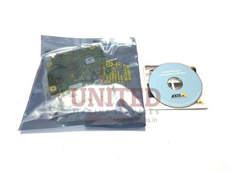
A barebone PCB, also known as a skeleton PCB or a minimal PCB, is a printed circuit board that contains only the essential components required for a specific function. Unlike a fully populated PCB, which includes all the necessary components and circuitry, a barebone PCB is designed to be customizable and adaptable to various applications.
Barebone PCBs are commonly used in electronics prototyping, testing, and small-scale production. They provide a cost-effective and time-efficient solution for engineers and hobbyists who want to create custom electronic devices without the need for a fully populated PCB.
Advantages of using Barebone PCBs
- Cost-effective: Barebone PCBs are less expensive than fully populated PCBs because they contain fewer components and require less assembly time.
- Customizable: Users can add or remove components as needed, making barebone PCBs highly adaptable to various applications.
- Time-efficient: With fewer components to assemble, barebone PCBs can be put together quickly, allowing for faster prototyping and testing.
- Compact: Barebone PCBs are usually smaller than fully populated PCBs, making them suitable for space-constrained applications.
Types of Barebone PCBs
There are several types of barebone PCBs available, each designed for specific applications and industries. Some common types include:
- Single-Sided PCBs: These PCBs have conductive traces on only one side of the board, making them the simplest and most cost-effective option.
- Double-sided PCBs: With conductive traces on both sides of the board, double-sided PCBs offer more flexibility and higher component density than single-sided PCBs.
- Multilayer PCBs: These PCBs consist of multiple layers of conductive traces, allowing for even higher component density and more complex designs.
- Flexible PCBs: Made from flexible materials, these PCBs can bend and conform to various shapes, making them ideal for wearable electronics and applications with limited space.
- Rigid-flex PCBs: A combination of rigid and flexible PCBs, these boards offer the benefits of both types, allowing for more complex designs and improved reliability.
Comparison of Barebone PCB Types
| PCB Type | Layers | Flexibility | Cost | Component Density |
|---|---|---|---|---|
| Single-sided | 1 | Rigid | Low | Low |
| Double-sided | 2 | Rigid | Medium | Medium |
| Multilayer | 3+ | Rigid | High | High |
| Flexible | 1-2 | Flexible | Medium | Low |
| Rigid-Flex | 2+ | Both | High | High |

How to Use Barebone PCBs
Using a barebone PCB involves several steps, from designing the circuit to assembling the components. Here’s a general overview of the process:
1. Circuit Design
The first step in using a barebone PCB is to design the circuit. This involves creating a schematic diagram that shows the connections between the various components. You can use electronic design automation (EDA) software, such as KiCad or Eagle, to create the schematic.
Tips for designing circuits for Barebone PCBs
- Keep the design simple and modular to make it easier to customize and adapt.
- Use standard component packages and footprints to ensure compatibility with available components.
- Consider the power requirements and heat dissipation of the components when designing the circuit.
2. PCB Layout
Once the schematic is complete, the next step is to create the PCB layout. This involves arranging the components on the board and routing the traces to connect them according to the schematic. EDA software is also used for this step, and it’s important to follow best practices for PCB layout to ensure optimal performance and reliability.
Best practices for PCB layout
- Use an appropriate grid size and trace width for the components and current requirements.
- Keep sensitive signals, such as high-speed digital lines or analog signals, away from noisy components or power traces.
- Provide adequate clearance between components and traces to avoid short circuits and manufacturability issues.
- Use ground planes and power planes to reduce EMI and improve signal integrity.
3. PCB Fabrication
After the PCB layout is finalized, the next step is to fabricate the barebone PCB. This involves sending the design files (usually Gerber files) to a PCB manufacturer, who will produce the physical board according to the specifications.
Choosing a PCB manufacturer
When selecting a PCB manufacturer, consider the following factors:
- Experience and reputation in the industry
- Capabilities and materials offered (e.g., board thickness, copper weight, surface finishes)
- Turnaround time and pricing
- Quality control and certifications (e.g., ISO, UL, RoHS)
4. Component Selection and Procurement
While the barebone PCB is being fabricated, you can start selecting and procuring the components needed for the design. This involves comparing specifications, prices, and availability from various suppliers and ensuring that the components are compatible with the barebone PCB.
Tips for component selection
- Use reputable suppliers with good track records for quality and reliability.
- Consider the lead time and minimum order quantities when planning the procurement.
- Verify the component specifications and packaging to ensure compatibility with the PCB design.
5. PCB Assembly
Once the barebone PCB and components are ready, the final step is to assemble the board. This involves soldering the components onto the PCB according to the schematic and layout. You can either assemble the board manually using soldering tools or use automated assembly services for larger quantities.
PCB assembly methods
| Method | Description | Advantages | Disadvantages |
|---|---|---|---|
| Hand soldering | Manually soldering components using a soldering iron | Low cost, flexible, suitable for small quantities | Time-consuming, requires skill, prone to human error |
| Reflow soldering | Using a reflow oven to solder surface mount components | Fast, consistent, suitable for medium to large quantities | Higher setup cost, limited to surface mount components |
| Wave soldering | Using a wave soldering machine to solder through-hole components | Fast, consistent, suitable for large quantities | Higher setup cost, limited to through-hole components |
Tips for PCB assembly
- Use appropriate soldering techniques and tools for the component types and sizes.
- Follow the manufacturer’s recommendations for soldering temperature and time.
- Inspect the assembled board for any defects, such as bridging, cold joints, or missing components.
- Clean the board after assembly to remove flux residue and improve appearance.

Applications of Barebone PCBs
Barebone PCBs find applications in various industries and projects, including:
- Prototyping and testing: Barebone PCBs are ideal for quickly testing new circuit designs and validating concepts before committing to a fully populated PCB.
- Custom electronic devices: Hobbyists and engineers can use barebone PCBs to create custom electronic devices tailored to their specific needs and requirements.
- Education and learning: Barebone PCBs are often used in educational settings to teach students about electronics and PCB design.
- Small-scale production: For low-volume production runs, barebone PCBs can be a cost-effective alternative to fully populated PCBs.

Frequently Asked Questions (FAQ)
- What is the difference between a barebone PCB and a fully populated PCB?
-
A barebone PCB contains only the essential components required for a specific function, while a fully populated PCB includes all the necessary components and circuitry for a complete electronic device.
-
Can I use a barebone PCB for high-volume production?
-
While barebone PCBs can be used for small-scale production, they may not be the most cost-effective option for high-volume production. In such cases, fully populated PCBs are generally more suitable.
-
What skills do I need to use a barebone PCB?
-
To use a barebone PCB effectively, you should have a basic understanding of electronics, circuit design, PCB layout, and soldering. Familiarity with EDA software and PCB assembly techniques is also helpful.
-
How do I choose the right barebone PCB for my project?
-
When selecting a barebone PCB, consider factors such as the required number of layers, flexibility, component density, and cost. Evaluate your project requirements and choose the type of barebone PCB that best meets your needs.
-
Can I modify a barebone PCB after assembly?
- Yes, one of the advantages of barebone PCBs is that they can be modified after assembly. You can add, remove, or replace components as needed to adapt the board to different applications or requirements.
Conclusion
Barebone PCBs offer a versatile and cost-effective solution for electronics prototyping, testing, and small-scale production. By understanding the different types of barebone PCBs, the design and assembly process, and their applications, engineers and hobbyists can leverage these boards to create custom electronic devices tailored to their specific needs.
As the electronics industry continues to evolve, barebone PCBs will remain an essential tool for innovation and experimentation. By staying up-to-date with the latest trends and techniques in barebone PCB design and assembly, users can unlock new possibilities and push the boundaries of what’s possible in the world of electronics.
No responses yet