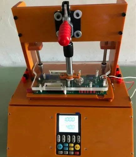
Introduction to PCB Testing Boards
A printed circuit board (PCB) testing board, also known as a programming jig or test fixture, is an essential tool for electronics manufacturers to program and test PCBs after assembly. A well-designed PCB testing board can greatly improve programming and testing efficiency, reduce errors, and ensure the quality and reliability of the final product.
In this article, we will discuss 14 tips on how to design an effective PCB Programming and testing board. By following these guidelines, you can create a testing board that meets your specific needs and streamlines your programming and testing process.
Tip 1: Determine the Purpose and Requirements
Before starting the design process, clearly define the purpose and requirements of your PCB testing board. Consider the following factors:
- The type and number of PCBs to be programmed and tested
- The programming and testing equipment to be used
- The required programming and testing functions
- The desired speed and accuracy of programming and testing
- The available budget and timeline for designing and manufacturing the testing board
By having a clear understanding of your needs and constraints, you can make informed decisions throughout the design process and ensure that your final product meets your expectations.

Tip 2: Choose the Right Connector Type
One of the most critical components of a PCB testing board is the connector that interfaces with the PCB under test. There are several types of connectors commonly used in testing boards, each with its advantages and disadvantages. Here are some popular options:
| Connector Type | Pros | Cons |
|---|---|---|
| Pogo Pins | – High reliability and durability | – Higher cost compared to other options |
| – Suitable for high-volume production | – Requires precise alignment | |
| – Allows for easy replacement of worn pins | ||
| Edge Connector | – Low cost and simple design | – Limited to PCBs with matching edge fingers |
| – Suitable for low-volume production | – Prone to wear and damage over time | |
| – Easy to align and connect | ||
| Bed of Nails | – Can accommodate PCBs with irregular shapes | – Higher cost and complexity |
| – Allows for testing multiple points at once | – Requires custom design for each PCB | |
| – Suitable for high-volume production | – Prone to wear and damage over time |
Choose the connector type that best suits your needs based on factors such as cost, durability, ease of use, and compatibility with your PCBs and testing equipment.

Tip 3: Ensure Proper Alignment and Contact
Proper alignment and contact between the PCB testing board and the PCB under test are crucial for accurate and reliable programming and testing. Here are some tips to ensure proper alignment and contact:
- Use guide pins, alignment holes, or other mechanical features to precisely align the PCB with the testing board
- Ensure that the connectors on the testing board and the PCB are compatible and properly sized
- Use spring-loaded pins or other compliant contact methods to accommodate variations in PCB Thickness and flatness
- Provide adequate contact force to ensure reliable electrical connections without damaging the PCB or the testing board
- Consider using vision systems or other automated alignment methods for high-volume production

Tip 4: Minimize Signal Interference and Crosstalk
Signal integrity is essential for accurate and reliable programming and testing. To minimize signal interference and crosstalk, follow these guidelines:
- Keep signal traces as short and direct as possible to reduce inductance and capacitance
- Use proper grounding and shielding techniques to reduce electromagnetic interference (EMI) and radio frequency interference (RFI)
- Separate sensitive signals from noisy signals, such as power lines and high-speed digital lines
- Use appropriate termination and impedance matching techniques to reduce reflections and ringing
- Follow the PCB layout guidelines and best practices for your specific application and test equipment
Tip 5: Incorporate Adequate ESD Protection
Electrostatic discharge (ESD) can cause damage to sensitive electronic components during programming and testing. To protect your PCBs and testing equipment from ESD, incorporate the following measures:
- Use ESD-safe materials and coatings for the testing board and its components
- Provide proper grounding paths for ESD currents to dissipate safely
- Use ESD protection devices, such as transient voltage suppressors (TVS) and gas discharge tubes (GDT), on sensitive signal lines
- Follow ESD-safe handling procedures, such as wearing ESD wrist straps and using ESD-safe workstations
- Regularly inspect and maintain ESD protection equipment to ensure its effectiveness
Tip 6: Plan for Scalability and Flexibility
As your product line evolves and your production volume increases, your PCB testing board should be able to adapt to changing needs. To plan for scalability and flexibility, consider the following:
- Design the testing board with modular or interchangeable components that can be easily updated or replaced
- Use standardized interfaces and protocols that are compatible with a wide range of PCBs and testing equipment
- Provide extra capacity and functionality to accommodate future expansion and upgrades
- Consider using automated or semi-automated testing methods that can be easily scaled up or down based on production volume
- Plan for regular maintenance and calibration to ensure the long-term reliability and accuracy of the testing board
Tip 7: Optimize for Speed and Efficiency
In high-volume production, the speed and efficiency of programming and testing can have a significant impact on overall throughput and cost. To optimize your PCB testing board for speed and efficiency, consider the following:
- Use high-speed programming and testing equipment that can handle the required data rates and volumes
- Minimize the number of manual operations and interventions required during the programming and testing process
- Use parallel programming and testing methods to process multiple PCBs simultaneously
- Implement automated handling and conveying systems to minimize the time and labor required for loading and unloading PCBs
- Use software tools and scripts to automate repetitive tasks and data analysis
Tip 8: Ensure Adequate Cooling and Ventilation
During programming and testing, the PCB and the testing board may generate significant amounts of heat that can affect their performance and reliability. To ensure adequate cooling and ventilation, follow these guidelines:
- Use heat sinks, fans, or other cooling methods to dissipate heat from critical components
- Provide adequate spacing and airflow around the testing board and the PCB to allow for natural convection cooling
- Use temperature sensors and monitoring systems to detect and alert for overheating conditions
- Consider using conformal coatings or other protective measures to prevent dust and debris from accumulating on the testing board and the PCB
- Plan for regular cleaning and maintenance to ensure the long-term performance and reliability of the cooling and ventilation system
Tip 9: Incorporate User-Friendly Features
A user-friendly PCB testing board can reduce operator errors, improve productivity, and enhance the overall user experience. Consider incorporating the following user-friendly features:
- Use clear and intuitive labeling and color-coding for connectors, switches, and indicators
- Provide visual and audible feedback for important events, such as successful programming or testing, errors, and warnings
- Use ergonomic designs and layouts that minimize physical strain and fatigue for the operator
- Provide easy access to frequently used controls and interfaces
- Use software tools and graphical user interfaces (GUIs) to simplify and automate complex tasks
Tip 10: Plan for Manufacturing and Assembly
The manufacturability and assemblability of your PCB testing board can have a significant impact on its cost, lead time, and quality. To plan for manufacturing and assembly, consider the following:
- Use standard components and materials that are readily available and cost-effective
- Minimize the number of custom or specialized parts that require additional tooling or processing
- Use design for manufacturing (DFM) and design for assembly (DFA) principles to optimize the layout and routing of the testing board
- Provide clear and comprehensive documentation, including bill of materials (BOM), assembly drawings, and fabrication files
- Work closely with your manufacturing and assembly partners to ensure that your design meets their capabilities and requirements
Tip 11: Conduct Thorough Testing and Validation
Before using your PCB testing board in production, it is essential to conduct thorough testing and validation to ensure its functionality, reliability, and compatibility. Here are some steps to follow:
- Develop a comprehensive test plan that covers all the required programming and testing functions and scenarios
- Use known good PCBs and known bad PCBs to validate the accuracy and consistency of the testing board
- Conduct stress tests and environmental tests to ensure the durability and reliability of the testing board under various conditions
- Verify the compatibility and interoperability of the testing board with your programming and testing equipment and software
- Document and analyze the test results to identify any issues or areas for improvement
Tip 12: Provide Comprehensive Documentation
Comprehensive documentation is essential for the proper use, maintenance, and troubleshooting of your PCB testing board. Include the following types of documentation:
- User manuals and quick start guides that provide clear and concise instructions for setting up and using the testing board
- Technical specifications and datasheets that describe the electrical, mechanical, and environmental characteristics of the testing board
- Schematics, board layouts, and assembly drawings that provide detailed information about the design and construction of the testing board
- Test reports and validation results that demonstrate the performance and reliability of the testing board
- Maintenance and calibration procedures that ensure the long-term accuracy and consistency of the testing board
Tip 13: Plan for Maintenance and Upgrades
A PCB testing board is a long-term investment that requires regular maintenance and upgrades to ensure its continued performance and relevance. Plan for the following:
- Develop a maintenance schedule that includes regular cleaning, inspection, and calibration of the testing board and its components
- Keep spare parts and consumables on hand to minimize downtime and repair costs
- Monitor the performance and reliability of the testing board over time to identify any trends or issues that may require attention
- Plan for upgrades and enhancements to the testing board as your needs and technologies evolve
- Work with your suppliers and partners to ensure the long-term availability and support of the testing board and its components
Tip 14: Consider Cost and Return on Investment
Designing and manufacturing a PCB testing board requires a significant investment of time, resources, and money. To ensure a positive return on investment (ROI), consider the following:
- Conduct a cost-benefit analysis to compare the costs of designing and manufacturing the testing board with the expected benefits, such as reduced programming and testing time, improved quality and reliability, and increased production throughput
- Look for opportunities to reuse or repurpose existing equipment and components to reduce the upfront costs of the testing board
- Consider the long-term costs of maintenance, upgrades, and support when evaluating the total cost of ownership (TCO) of the testing board
- Work with your finance and accounting teams to develop a business case and financial justification for the testing board project
- Monitor the actual costs and benefits of the testing board over time to validate your assumptions and make data-driven decisions about future investments
FAQ
Q1: What is a PCB testing board, and why is it important?
A: A PCB testing board, also known as a programming jig or test fixture, is a specialized device used to program and test printed circuit boards (PCBs) after assembly. It is important because it enables electronics manufacturers to ensure the quality, functionality, and reliability of their PCBs before shipping them to customers. A well-designed PCB testing board can greatly improve programming and testing efficiency, reduce errors and rework, and ultimately save time and money in the production process.
Q2: What are some common types of connectors used in PCB testing boards?
A: Some common types of connectors used in PCB testing boards include:
- Pogo pins: Spring-loaded pins that provide high reliability and durability, suitable for high-volume production
- Edge connectors: Low-cost and simple connectors that interface with matching edge fingers on the PCB, suitable for low-volume production
- Bed of nails: Custom-designed connectors that can accommodate PCBs with irregular shapes and test multiple points simultaneously, suitable for high-volume production
The choice of connector type depends on factors such as cost, durability, ease of use, and compatibility with the PCBs and testing equipment.
Q3: How can I ensure proper alignment and contact between the PCB testing board and the PCB under test?
A: To ensure proper alignment and contact, you can use the following techniques:
- Use guide pins, alignment holes, or other mechanical features to precisely align the PCB with the testing board
- Ensure that the connectors on the testing board and the PCB are compatible and properly sized
- Use spring-loaded pins or other compliant contact methods to accommodate variations in PCB thickness and flatness
- Provide adequate contact force to ensure reliable electrical connections without damaging the PCB or the testing board
- Consider using vision systems or other automated alignment methods for high-volume production
Q4: What are some ways to minimize signal interference and crosstalk in a PCB testing board?
A: To minimize signal interference and crosstalk, you can follow these guidelines:
- Keep signal traces as short and direct as possible to reduce inductance and capacitance
- Use proper grounding and shielding techniques to reduce electromagnetic interference (EMI) and radio frequency interference (RFI)
- Separate sensitive signals from noisy signals, such as power lines and high-speed digital lines
- Use appropriate termination and impedance matching techniques to reduce reflections and ringing
- Follow the PCB layout guidelines and best practices for your specific application and test equipment
Q5: How can I optimize my PCB testing board for speed and efficiency in high-volume production?
A: To optimize your PCB testing board for speed and efficiency in high-volume production, you can consider the following:
- Use high-speed programming and testing equipment that can handle the required data rates and volumes
- Minimize the number of manual operations and interventions required during the programming and testing process
- Use parallel programming and testing methods to process multiple PCBs simultaneously
- Implement automated handling and conveying systems to minimize the time and labor required for loading and unloading PCBs
- Use software tools and scripts to automate repetitive tasks and data analysis
By following these tips and continuously monitoring and improving your programming and testing process, you can achieve significant gains in speed, efficiency, and overall productivity.
Conclusion
Designing a PCB programming and testing board is a complex and iterative process that requires careful planning, execution, and optimization. By following the 14 tips outlined in this article, you can create a testing board that meets your specific needs, ensures the quality and reliability of your PCBs, and maximizes your return on investment.
Remember to start with a clear understanding of your requirements and constraints, choose the right components and design techniques, and plan for scalability, flexibility, and long-term maintenance. By collaborating with your team and partners, conducting thorough testing and validation, and providing comprehensive documentation, you can ensure the success and longevity of your PCB testing board.
As technology and market demands continue to evolve, it is essential to stay up-to-date with the latest trends, best practices, and innovations in PCB programming and testing. By continuously learning, adapting, and improving your processes and tools, you can stay ahead of the competition and deliver high-quality products to your customers.
No responses yet