Introduction to PCB Gold Fingers
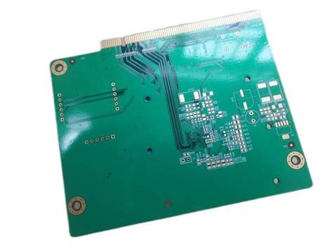
PCB gold fingers, also known as edge connectors or contact fingers, are the gold-plated contacts on the edge of a printed circuit board (PCB). These gold-plated contacts are designed to provide a reliable and durable electrical connection between the PCB and other components or devices. Gold fingers are commonly found on various types of PCBs, including computer memory modules, graphics cards, and expansion cards.
What are PCB Gold Fingers?
PCB gold fingers are the exposed, gold-plated contacts on the edge of a PCB that allow it to be plugged into a connector or socket. These contacts are typically arranged in a specific pattern to ensure proper alignment and connection with the mating connector. Gold is used as the plating material because of its excellent electrical conductivity, corrosion resistance, and durability.
Importance of Gold Fingers in PCBs
Gold fingers play a crucial role in ensuring reliable electrical connections between PCBs and other components. Some of the key reasons why gold fingers are essential in PCBs include:
- High conductivity: Gold is an excellent conductor of electricity, which ensures minimal signal loss and optimal performance.
- Corrosion resistance: Gold is resistant to oxidation and corrosion, which helps maintain the integrity of the electrical connections over time.
- Durability: Gold-plated contacts can withstand multiple insertion and removal cycles without significant wear or damage.
- Low contact resistance: Gold fingers provide low contact resistance, which is essential for high-speed and high-frequency applications.
PCB Gold Finger Plating Process
The process of creating gold fingers on a PCB involves several steps, including surface preparation, plating, and finishing. Let’s take a closer look at each stage of the PCB gold finger plating process.
Surface Preparation
Before the gold plating can be applied, the PCB surface must be properly prepared to ensure good adhesion and uniform coverage. The surface preparation process typically involves the following steps:
- Cleaning: The PCB surface is cleaned to remove any dirt, grease, or contaminants that could interfere with the plating process.
- Roughening: The contact area is mechanically or chemically roughened to increase the surface area and improve adhesion of the plating.
- Activation: The surface is treated with a special solution to activate the copper and promote the formation of a strong bond with the plating material.
Plating Process
Once the surface is prepared, the actual plating process can begin. The PCB gold finger plating process typically involves the following steps:
- Nickel plating: A layer of nickel is first plated onto the copper surface to provide a barrier between the copper and the gold. This helps prevent the formation of intermetallic compounds that can weaken the bond between the two metals.
- Gold plating: A layer of gold is then plated onto the nickel surface. The thickness of the gold layer can vary depending on the specific requirements of the application, but it typically ranges from 0.05 to 0.5 micrometers.
- Inspection: After plating, the gold fingers are inspected to ensure proper coverage, thickness, and adhesion.
Finishing and Protection
After the gold plating process is complete, the PCB may undergo additional finishing and protection steps to enhance its durability and performance. These steps may include:
- Solder mask application: A solder mask is applied to the PCB to protect the non-contact areas from oxidation and prevent solder bridging during assembly.
- Surface finish: An additional surface finish, such as immersion gold or organic solderability preservative (OSP), may be applied to the gold fingers to improve solderability and protect against contamination.
- Packaging: The finished PCBs are packaged in antistatic materials to protect them from damage and contamination during storage and transportation.

Advantages of PCB Gold Fingers
PCB gold fingers offer several advantages over other contact materials and plating processes. Some of the key benefits include:
- Excellent electrical conductivity: Gold is one of the best conductors of electricity, which ensures minimal signal loss and optimal performance in high-speed and high-frequency applications.
- High durability: Gold-plated contacts can withstand thousands of insertion and removal cycles without significant wear or damage, making them ideal for applications that require frequent plugging and unplugging.
- Corrosion resistance: Gold is resistant to oxidation and corrosion, which helps maintain the integrity of the electrical connections over time, even in harsh environments.
- Compatibility with lead-free soldering: Gold is compatible with lead-free soldering processes, which are becoming increasingly common in the electronics industry due to environmental and health concerns.

Challenges and Considerations in PCB Gold Finger Plating
While PCB gold finger plating offers many benefits, there are also some challenges and considerations that must be taken into account during the design and manufacturing process. These include:
- Cost: Gold is a relatively expensive material, which can increase the overall cost of the PCB. However, the added cost is often justified by the improved performance and reliability of the gold-plated contacts.
- Plating thickness: The thickness of the gold plating must be carefully controlled to ensure optimal performance and durability. If the plating is too thin, it may not provide sufficient protection against wear and corrosion. If it is too thick, it can cause issues with solderability and insertion forces.
- Design considerations: The layout and spacing of the gold fingers must be carefully designed to ensure proper alignment and connection with the mating connector. The design must also take into account the specific requirements of the application, such as signal integrity, impedance matching, and mechanical stress.

Applications of PCB Gold Fingers
PCB gold fingers are used in a wide range of applications across various industries. Some of the most common applications include:
- Computer memory modules: Gold fingers are used on memory modules, such as DIMMs and SIMMs, to provide a reliable connection between the module and the motherboard.
- Graphics cards and expansion cards: High-performance graphics cards and other expansion cards often use gold fingers to ensure optimal signal integrity and durability.
- Telecommunications equipment: Gold fingers are used in various telecommunications equipment, such as routers and switches, to provide reliable connections between PCBs and backplanes.
- Industrial and automotive electronics: Gold fingers are used in industrial and automotive applications that require high reliability and durability, such as sensors, controllers, and diagnostic tools.
- Medical devices: Gold fingers are used in medical devices that require stable and reliable electrical connections, such as patient monitors and diagnostic equipment.
Frequently Asked Questions (FAQ)
-
What is the difference between gold fingers and edge connectors?
Gold fingers and edge connectors are essentially the same things. Gold fingers refer specifically to the gold-plated contacts on the edge of a PCB, while edge connectors refer to the overall design of the PCB edge that allows it to be plugged into a connector or socket. -
How thick should the gold plating be on PCB fingers?
The thickness of the gold plating on PCB fingers can vary depending on the specific requirements of the application. Typical thicknesses range from 0.05 to 0.5 micrometers (2 to 20 microinches). Thicker plating may be required for applications that involve frequent plugging and unplugging or exposure to harsh environments. -
Can other materials be used instead of gold for PCB fingers?
While gold is the most common material used for PCB fingers due to its excellent electrical and mechanical properties, other materials, such as palladium or silver, can also be used in some applications. However, these materials may not provide the same level of durability and corrosion resistance as gold. -
How do I specify the gold finger design for my PCB?
When designing a PCB with gold fingers, you should specify the number of fingers, the pitch (spacing between fingers), the length and width of the fingers, and the thickness of the gold plating. You should also provide information about the mating connector or socket to ensure proper alignment and compatibility. -
How can I test the quality of PCB gold fingers?
There are several methods for testing the quality of PCB gold fingers, including visual inspection, dimensional measurement, plating thickness measurement, and contact resistance testing. Visual inspection can help identify any defects or irregularities in the plating, while dimensional measurement ensures that the fingers meet the specified size and spacing requirements. Plating thickness can be measured using X-ray fluorescence (XRF) or cross-sectioning techniques, and contact resistance can be tested using a four-wire resistance measurement method.
Conclusion
PCB gold fingers play a critical role in ensuring reliable and durable electrical connections between PCBs and other components. The gold plating process involves careful surface preparation, plating, and finishing to achieve optimal performance and longevity. While gold fingers offer many advantages, such as excellent conductivity and corrosion resistance, they also present some challenges and considerations in terms of cost, design, and manufacturing.
By understanding the basics of PCB gold fingers and the plating process, engineers and designers can make informed decisions when specifying and designing PCBs for various applications. With proper design, manufacturing, and testing, PCB gold fingers can provide reliable and high-performance electrical connections for a wide range of products and industries.
No responses yet