Introduction to PCB Trace Width and Current
When designing a printed circuit board (PCB), one of the crucial aspects to consider is the width of the traces and the current they can handle. Properly sizing the traces ensures reliable operation, prevents overheating, and minimizes voltage drop. In this article, we will delve into the factors that influence PCB trace width and current, provide guidelines for calculating the appropriate trace dimensions, and answer frequently asked questions.
Factors Affecting PCB Trace Width and Current
Several factors come into play when determining the appropriate trace width and current for a PCB. These include:
Current Requirements
The amount of current a trace needs to carry is a primary factor in determining its width. Higher currents require wider traces to prevent excessive heating and voltage drop.
Temperature Rise
As current flows through a trace, it generates heat. The temperature rise of the trace depends on the current, trace width, and the PCB’s ability to dissipate heat. Excessive temperature rise can lead to reliability issues and damage to the PCB.
Voltage Drop
When current flows through a trace, there is a voltage drop due to the trace’s resistance. This voltage drop can affect the performance of the connected components. Wider traces have lower resistance and, consequently, lower voltage drop.
PCB Material and Thickness
The choice of PCB material and its thickness also influence trace width and current. Different materials have varying thermal conductivity and current-carrying capacity. Thicker PCBs can dissipate heat more effectively, allowing for higher current densities.

Calculating PCB Trace Width
To calculate the appropriate trace width for a given current, you can use the following formula:
Trace Width (mils) = (Current (A) / (k * (ΔT)^b))^(1/c)
Where:
– Current (A) is the maximum current the trace needs to carry in amperes.
– k, b, and c are constants that depend on the PCB material and thickness.
– ΔT is the allowed temperature rise above ambient in °C.
The values of k, b, and c can be found in the IPC-2152 standard, which provides guidelines for determining current-carrying capacity of conductors for printed boards.
Here’s an example table of k, b, and c values for different copper thicknesses:
| Copper Thickness (oz) | k | b | c |
|---|---|---|---|
| 0.5 | 0.048 | 0.44 | 0.725 |
| 1 | 0.024 | 0.44 | 0.725 |
| 2 | 0.012 | 0.44 | 0.725 |
| 3 | 0.008 | 0.44 | 0.725 |
To use the formula, follow these steps:
1. Determine the maximum current the trace needs to carry.
2. Choose the appropriate values of k, b, and c based on the PCB material and copper thickness.
3. Decide on the allowed temperature rise (ΔT) based on the PCB’s operating environment and component tolerances.
4. Plug the values into the formula and calculate the trace width.
For example, let’s say you have a 1 oz copper PCB, and you need to route a trace carrying 2A with an allowed temperature rise of 10°C. Using the values from the table, the calculation would be:
Trace Width (mils) = (2 / (0.024 * (10)^0.44))^(1/0.725) ≈ 103 mils
This means that to carry 2A with a temperature rise of 10°C, the trace should be approximately 103 mils wide.

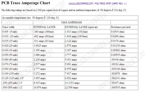
PCB Trace Current Capacity Tables
To simplify the process of determining trace widths, you can refer to pre-calculated tables that provide the current-carrying capacity for various trace widths and copper thicknesses. Here’s an example table for 1 oz copper:
| Trace Width (mils) | Current Capacity (A) |
|---|---|
| 10 | 0.5 |
| 20 | 1.0 |
| 50 | 2.5 |
| 100 | 4.0 |
| 150 | 6.0 |
| 200 | 8.0 |
These values assume a temperature rise of 10°C above ambient. If your design requires a different temperature rise or copper thickness, you can find more comprehensive tables in the IPC-2152 standard or use the trace width formula.

Frequently Asked Questions (FAQ)
1. What happens if the trace width is too narrow for the current?
If a trace is too narrow for the current it carries, it can lead to several problems:
– Excessive heating: The trace may heat up beyond its rated temperature, causing damage to the PCB and connected components.
– Voltage drop: Narrow traces have higher resistance, resulting in a larger voltage drop along the trace. This can affect the performance of the connected components.
– Reliability issues: Overheating and voltage drop can cause intermittent behavior, signal integrity problems, and even permanent damage to the PCB.
2. Can I use different trace widths for different sections of the same net?
Yes, you can use different trace widths for different sections of the same net. This is called “necking down.” It is common to use wider traces for high-current sections and narrower traces for low-current sections or where space is limited. However, when necking down, ensure that the narrowest section can still handle the required current.
3. How does the PCB’s ambient temperature affect trace width calculations?
The ambient temperature of the PCB’s operating environment affects the trace width calculations. Higher ambient temperatures mean that the trace has less room for temperature rise before reaching its limit. In such cases, you may need to use wider traces to compensate for the reduced temperature headroom.
4. What is the impact of using thicker copper on trace width?
Using thicker copper allows for narrower traces while maintaining the same current-carrying capacity. This is because thicker copper has lower resistance and can dissipate heat more effectively. For example, a 2 oz copper trace can be narrower than a 1 oz copper trace carrying the same current.
5. Can I use online calculators or software to determine trace widths?
Yes, there are many online calculators and PCB design software that can help you determine the appropriate trace widths for your design. These tools often have built-in trace width calculators that take into account factors like current, temperature rise, and copper thickness. However, it’s essential to verify the results and ensure they meet your specific design requirements.
Conclusion
Determining the appropriate PCB trace width and current is crucial for ensuring reliable operation, preventing overheating, and minimizing voltage drop. By understanding the factors that influence trace width and current, using the provided formula or reference tables, and following best practices, you can design PCBs that meet your performance and reliability requirements.
Remember to consider the specific needs of your design, such as the PCB material, copper thickness, ambient temperature, and allowed temperature rise. When in doubt, consult the IPC-2152 standard or seek guidance from experienced PCB designers.
By properly sizing your PCB traces, you can create robust and efficient designs that stand the test of time.
No responses yet