Introduction to PCB Prototypes
Printed Circuit Board (PCB) prototypes are essential for testing and validating the design of electronic circuits before mass production. PCB Prototyping allows engineers and designers to identify and fix any issues with the circuit design, component layout, and manufacturability of the board. In this article, we will explore the process of manufacturing and assembling PCB prototypes, focusing on the 3+3 approach.
What is the 3+3 Approach to PCB Prototyping?
The 3+3 approach to PCB prototyping involves creating three bare PCBs and three assembLED PCBs. This method provides a balance between cost-effectiveness and the ability to test the PCB design thoroughly. Here’s a breakdown of the 3+3 approach:
- Three bare PCBs:
- Used for visual inspection and dimensional verification
- Allows for testing of the PCB material and copper traces
-
Provides a backup in case of assembly issues
-
Three assembled PCBs:
- Used for functional testing and validation of the circuit design
- Allows for testing of component placement and soldering quality
- Provides a backup in case of component failure or assembly issues

The PCB Prototyping Process
Step 1: PCB Design and Layout
The first step in creating PCB prototypes is to design the circuit schematic and layout the PCB using electronic design automation (EDA) software. Some popular EDA tools include:
- Altium Designer
- KiCad
- Eagle PCB
- OrCAD
During the design process, engineers must consider factors such as:
- Component selection and placement
- Signal integrity and electromagnetic compatibility (EMC)
- Power distribution and thermal management
- Manufacturing constraints and design for manufacturability (DFM)
Step 2: Generating Gerber Files
Once the PCB design is complete, the next step is to generate Gerber files. Gerber files are the industry standard format for describing the layout of a PCB, including the copper layers, solder mask, silkscreen, and drill holes. The Gerber files are used by PCB manufacturers to fabricate the bare PCBs.
Step 3: PCB Fabrication
PCB fabrication involves the following steps:
- Printing the circuit pattern onto a photosensitive film
- Laminating the copper-clad board with the photosensitive film
- Exposing the board to UV light to harden the photoresist
- Developing the board to remove the unhardened photoresist
- Etching away the unwanted copper to create the circuit traces
- Applying a solder mask and silkscreen to protect the board and label components
- Drilling holes for through-hole components and vias
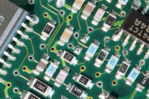
Step 4: PCB Assembly
After the bare PCBs are fabricated, the next step is to assemble the components onto the board. PCB assembly can be done manually for low-volume prototypes or using automated assembly lines for higher volumes. The assembly process typically involves the following steps:
- Applying solder paste to the PCB pads using a stencil
- Placing components onto the PCB using a pick-and-place machine or by hand
- Reflowing the solder paste in a reflow oven to permanently attach the components
- Inspecting the assembled PCB for defects and soldering quality
Step 5: PCB Testing and Validation
The final step in the PCB prototyping process is to test and validate the assembled PCBs. This involves:
-
Visual inspection: Checking for any visible defects, such as damaged components, solder bridges, or poor soldering quality.
-
Electrical testing: Verifying that the PCB functions as intended by testing its electrical characteristics, such as continuity, resistance, and voltage levels.
-
Functional testing: Testing the PCB in its intended application to ensure that it performs as expected under real-world conditions.
| Test Type | Description | Equipment | Purpose |
|---|---|---|---|
| Visual Inspection | Checking for visible defects | Microscope, magnifying glass | Identify manufacturing defects |
| Electrical Testing | Verifying electrical characteristics | Multimeter, oscilloscope, power supply | Ensure proper electrical functionality |
| Functional Testing | Testing PCB in intended application | Application-specific test equipment | Validate real-world performance |

Advantages of the 3+3 Approach
The 3+3 approach to PCB prototyping offers several advantages:
-
Cost-effectiveness: By manufacturing and assembling only three bare PCBs and three assembled PCBs, the 3+3 approach minimizes the cost of prototyping while still providing enough samples for thorough testing.
-
Risk mitigation: Having three assembled PCBs allows for testing redundancy and reduces the risk of a single faulty PCB derailing the entire testing process.
-
Design validation: The bare PCBs can be used to validate the PCB design, ensuring that the dimensions, hole sizes, and copper traces are correct before proceeding with assembly.
-
Flexibility: The 3+3 approach provides flexibility in testing, allowing engineers to use the bare PCBs for specific tests and the assembled PCBs for others, depending on the requirements of the project.

Choosing a PCB Prototyping Service
When selecting a PCB prototyping service, consider the following factors:
-
Manufacturing capabilities: Ensure that the service provider can manufacture PCBs with the required specifications, such as the number of layers, material type, and minimum feature size.
-
Assembly options: Check if the service provider offers assembly services, including surface mount technology (SMT) and through-hole assembly, and if they can source the required components.
-
Turnaround time: Consider the service provider’s turnaround time for both PCB fabrication and assembly, as this can impact your project timeline.
-
Quality control: Inquire about the service provider’s quality control processes, including their inspection and testing procedures, to ensure that you receive high-quality PCB prototypes.
-
Customer support: Look for a service provider with responsive and knowledgeable customer support, as this can be invaluable in case of any issues or questions during the prototyping process.
FAQ
Q1: What is the typical turnaround time for PCB prototypes?
A1: The turnaround time for PCB prototypes varies depending on the complexity of the design and the service provider. Typically, bare PCBs can be manufactured within 1-2 weeks, while assembled PCBs may take an additional 1-2 weeks. However, some service providers offer expedited manufacturing and assembly options for a higher cost.
Q2: How much does it cost to manufacture and assemble PCB prototypes?
A2: The cost of manufacturing and assembling PCB prototypes depends on several factors, such as the size of the PCB, the number of layers, the quantity, and the components used. As a rough estimate, a set of 3+3 PCB prototypes (three bare PCBs and three assembled PCBs) can cost anywhere from $500 to $2,000 or more, depending on the complexity of the design.
Q3: Can I assemble the PCB prototypes myself to save costs?
A3: Yes, you can assemble the PCB prototypes yourself to save on assembly costs. However, keep in mind that manual assembly requires skill, experience, and specialized equipment, such as a soldering iron, microscope, and tweezers. If you are not confident in your assembly skills, it may be more cost-effective and time-efficient to outsource the assembly to a professional service provider.
Q4: What files do I need to provide to a PCB prototyping service?
A4: To have your PCB prototypes manufactured and assembled, you typically need to provide the following files:
– Gerber files for PCB fabrication
– Bill of Materials (BOM) for component sourcing
– Pick-and-Place files for automated assembly
– Assembly drawings or instructions for manual assembly
Q5: How can I ensure the quality of my PCB prototypes?
A5: To ensure the quality of your PCB prototypes, consider the following:
– Use a reputable PCB prototyping service with a track record of delivering high-quality products
– Provide clear and accurate design files and specifications
– Conduct thorough testing and validation of the prototypes, including visual inspection, electrical testing, and functional testing
– Work closely with your PCB prototyping service provider and communicate any issues or concerns promptly
Conclusion
PCB prototyping is a critical step in the development of electronic products, allowing engineers and designers to test and validate their designs before proceeding with mass production. The 3+3 approach to PCB prototyping offers a cost-effective and flexible way to create prototypes for thorough testing and validation.
When selecting a PCB prototyping service, consider factors such as manufacturing capabilities, assembly options, turnaround time, quality control, and customer support. By working with a reputable service provider and following best practices for PCB design and testing, you can ensure that your PCB prototypes meet your requirements and help bring your electronic product to market successfully.
No responses yet