Key Features of PCB Visualizer
PCB Visualizer offers a range of features that enhance the PCB design workflow:
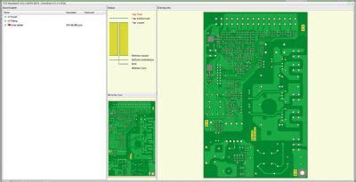
1. 3D Visualization
The primary feature of PCB Visualizer is its ability to render PCB designs in a realistic 3D environment. Users can zoom, rotate, and pan the PCB model to examine it from different angles and perspectives. This 3D visualization helps in understanding the spatial relationships between components, identifying potential issues, and communicating the design effectively to stakeholders.
2. Layer-by-Layer View
PCB Visualizer allows users to view the PCB design layer by layer. This feature is particularly useful for multi-layer PCBs, where understanding the placement and routing of traces on each layer is crucial. Users can toggle the visibility of individual layers, helping them focus on specific aspects of the design.
3. Component Placement and Orientation
The software provides a clear representation of component placement and orientation on the PCB. Users can select individual components to view their properties, such as part number, footprint, and electrical characteristics. This information helps in verifying the correctness of the component placement and ensuring compatibility with the overall design.
4. Trace Routing and Connectivity
PCB Visualizer enables users to trace the routing of signals and power traces on the PCB. It highlights the connections between components, making it easier to understand the signal flow and identify potential issues such as signal integrity problems or crosstalk. The software also provides tools for measuring trace lengths and analyzing impedance characteristics.
5. Design Rule Checking (DRC)
PCB Visualizer integrates with design rule checking (DRC) tools to validate the PCB design against a set of predefined rules and constraints. DRC helps identify issues such as minimum clearance violations, trace width violations, and component placement errors. By running DRC within PCB Visualizer, users can quickly identify and resolve design issues before proceeding to manufacturing.
6. Collaboration and Communication
PCB Visualizer facilitates collaboration and communication among team members involved in the PCB design process. The software allows users to add annotations, comments, and markups directly on the 3D model. These annotations can be shared with other team members, enabling effective communication and decision-making.
Benefits of Using PCB Visualizer
Using PCB Visualizer offers several benefits throughout the PCB design process:
1. Enhanced Design Understanding
The 3D visualization and layer-by-layer view provided by PCB Visualizer help designers and engineers gain a better understanding of the PCB design. They can easily comprehend the spatial relationships between components, the routing of traces, and the overall layout of the board. This enhanced understanding leads to more informed decision-making and reduces the likelihood of design errors.
2. Early Issue Detection
PCB Visualizer enables early detection of potential issues in the PCB design. By visually inspecting the 3D model and running design rule checks, users can identify problems such as component collisions, trace routing errors, and manufacturing constraints violations. Detecting and resolving these issues early in the design process saves time and reduces the cost of iterations.
3. Improved Communication
The collaboration features of PCB Visualizer streamline communication among team members. Designers, engineers, and stakeholders can add annotations and comments directly on the 3D model, making it easier to discuss design aspects, propose changes, and reach consensus. This improved communication reduces misunderstandings and ensures that everyone is aligned throughout the design process.
4. Faster Design Iterations
PCB Visualizer accelerates the design iteration process by providing instant feedback on design changes. Users can quickly modify the PCB Layout, component placement, or trace routing and immediately see the impact of those changes in the 3D environment. This real-time feedback allows for faster iterations and helps in optimizing the design.
5. Manufacturing Readiness
By using PCB Visualizer, designers can ensure that their PCB designs are ready for manufacturing. The software helps in identifying and resolving manufacturing-related issues, such as component clearance, trace width, and drill hole sizes. By addressing these issues early, the design can be optimized for manufacturing, reducing the risk of delays or costly rework.

PCB Visualizer Workflow
The typical workflow when using PCB Visualizer involves the following steps:
-
Import PCB Design: The PCB design files, typically in formats such as Gerber or ODB++, are imported into PCB Visualizer. The software reads the design data and generates a 3D model of the PCB.
-
Explore and Analyze: Users can explore the 3D model of the PCB, rotating, zooming, and panning to examine different aspects of the design. They can view the PCB layer by layer, select components to view their properties, and trace the routing of signals and power traces.
-
Design Rule Checking: PCB Visualizer integrates with design rule checking tools to validate the PCB design against predefined rules and constraints. Users can run DRC within the software to identify and resolve design issues.
-
Collaborate and Communicate: Team members can add annotations, comments, and markups directly on the 3D model to communicate design aspects, propose changes, and discuss issues. These annotations can be shared among team members for effective collaboration.
-
Iterate and Optimize: Based on the analysis and feedback obtained through PCB Visualizer, designers can make iterative changes to the PCB layout, component placement, or trace routing. The software provides instant feedback on these changes, allowing for faster iterations and design optimization.
-
Prepare for Manufacturing: Once the PCB design is finalized and optimized, users can use PCB Visualizer to ensure manufacturing readiness. They can verify that the design meets manufacturing constraints and make any necessary adjustments before proceeding to fabrication.

Integrating PCB Visualizer into the Design Process
To effectively integrate PCB Visualizer into the design process, consider the following best practices:
-
Start Early: Introduce PCB Visualizer early in the design process, preferably during the schematic capture and initial layout stages. This allows for early detection and resolution of design issues.
-
Collaborate with Stakeholders: Involve all relevant stakeholders, such as electrical engineers, mechanical engineers, and manufacturing experts, in the PCB Visualizer workflow. Encourage them to provide input and feedback using the collaboration features of the software.
-
Establish Design Standards: Define and document design standards and guidelines that align with the capabilities of PCB Visualizer. This ensures consistency and reduces the likelihood of design errors.
-
Regularly Review and Validate: Schedule regular design reviews using PCB Visualizer to assess the progress and integrity of the PCB design. Use the software’s analysis and validation features to identify and address any issues promptly.
-
Integrate with Other Tools: Ensure that PCB Visualizer integrates seamlessly with other tools in your design workflow, such as schematic capture software, simulation tools, and manufacturing preparation software. This streamlines the overall design process and reduces the risk of data inconsistencies.

PCB Visualizer and Industry Standards
PCB Visualizer supports various industry standards and file formats commonly used in PCB design and manufacturing. Some of the key standards and formats supported by PCB Visualizer include:
| Standard/Format | Description |
|---|---|
| Gerber | A widely used format for representing PCB Layers and manufacturing data. |
| ODB++ | A comprehensive PCB design and manufacturing data format that includes both design and fabrication information. |
| IPC-2581 | An industry standard for PCB design data exchange that encompasses design, fabrication, and assembly information. |
| STEP | A neutral file format for exchanging 3D CAD data, commonly used for mechanical integration of PCBs. |
By supporting these standards and formats, PCB Visualizer ensures compatibility with other tools in the PCB design and manufacturing ecosystem, enabling seamless data exchange and collaboration.
Frequently Asked Questions (FAQ)
1. Is PCB Visualizer suitable for both simple and complex PCB designs?
Yes, PCB Visualizer is versatile and can handle a wide range of PCB designs, from simple single-layer boards to complex multi-layer designs with high component density. The software’s features and capabilities scale well to accommodate different levels of complexity.
2. Can PCB Visualizer be used for flex and Rigid-Flex PCB designs?
Yes, PCB Visualizer supports the visualization and analysis of flex and Rigid-Flex PCB Designs. The software can accurately represent the unique characteristics of flexible and rigid-flex PCBs, such as bend regions and layer stackups.
3. Does PCB Visualizer integrate with popular PCB design software?
PCB Visualizer integrates with many popular PCB design software packages through standard file formats like Gerber and ODB++. This allows designers to seamlessly import their PCB designs into PCB Visualizer for visualization and analysis.
4. Can PCB Visualizer be used for collaboration with remote team members?
Yes, PCB Visualizer supports collaboration features that enable remote team members to view, annotate, and discuss PCB designs. The software allows users to share 3D models and annotations, facilitating effective communication and decision-making, regardless of the team’s physical location.
5. Is training available for PCB Visualizer?
Yes, training resources are available for PCB Visualizer. Many software providers offer online tutorials, video courses, and documentation to help users get started and master the features of the software. Additionally, some providers offer on-site or online training sessions for teams or individuals who require more personalized guidance.
Conclusion
PCB Visualizer is a powerful tool that revolutionizes the way PCB designs are viewed, analyzed, and understood. By providing a realistic 3D representation of PCBs, along with features like layer-by-layer view, component placement, trace routing, and design rule checking, PCB Visualizer enables designers, engineers, and stakeholders to make informed decisions throughout the design process.
The benefits of using PCB Visualizer are numerous, including enhanced design understanding, early issue detection, improved communication, faster design iterations, and manufacturing readiness. By integrating PCB Visualizer into the design workflow and following best practices, organizations can streamline their PCB design process, reduce errors, and accelerate time to market.
As PCB designs continue to increase in complexity and density, tools like PCB Visualizer become essential for managing the intricacies of modern electronics. By leveraging the capabilities of PCB Visualizer, designers and manufacturers can push the boundaries of innovation while ensuring the reliability and manufacturability of their PCB designs.
No responses yet