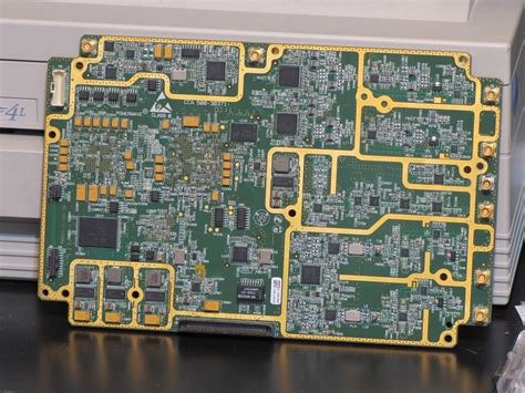
Introduction to RF-PCB
Radio Frequency Printed Circuit Boards (RF-PCBs) are specialized circuit boards designed to carry high-frequency signals with minimal loss and interference. These boards are crucial components in various applications, such as wireless communication devices, radar systems, and medical equipment. RF-PCBs require careful design considerations and manufacturing techniques to ensure optimal performance and reliability.
Key Characteristics of RF-PCBs
- High-frequency signal handling
- Controlled impedance
- Low dielectric loss
- Tight tolerances
- Specialized materials
RF-PCB Design Considerations
Designing RF-PCBs involves several critical factors that must be taken into account to ensure proper functionality and performance. Some of the key design considerations include:
Signal Integrity
Signal integrity is paramount in RF-PCB design. The layout must minimize signal reflections, crosstalk, and electromagnetic interference (EMI). This is achieved through careful trace routing, impedance matching, and the use of ground planes and shielding techniques.
Impedance Control
Maintaining consistent impedance throughout the RF signal path is essential for minimizing signal reflections and ensuring efficient power transfer. Controlled impedance is achieved by carefully selecting the dielectric material, substrate thickness, and trace dimensions.
Material Selection
The choice of substrate material is crucial for RF-PCBs. Materials with low dielectric loss, such as Rogers RO4000 series or Taconic RF-35, are commonly used to minimize signal attenuation and maintain signal integrity at high frequencies.
Grounding and Shielding
Proper grounding and shielding techniques are essential for minimizing EMI and ensuring signal quality. This includes the use of ground planes, via stitching, and shielding enclosures.

RF-PCB Manufacturing Process
Manufacturing RF-PCBs requires specialized processes and equipment to achieve the necessary precision and reliability. The manufacturing process typically involves the following steps:
- Material selection and preparation
- Photolithography
- Etching
- Plating
- Solder mask application
- Silkscreen printing
- Electrical testing and inspection
Material Selection and Preparation
The selected substrate material is cut to the desired size and cleaned to remove any contaminants. Copper foil is then laminated onto the substrate using heat and pressure.
Photolithography
The circuit pattern is transferred onto the copper-clad substrate using a photoresist and exposure to UV light. The exposed areas of the photoresist are then developed, leaving behind a protective layer in the desired circuit pattern.
Etching
The exposed copper areas are chemically etched away, leaving behind the desired circuit traces. Various etching techniques, such as wet etching or plasma etching, can be employed depending on the desired precision and production volume.
Plating
After etching, the remaining copper traces are often plated with additional metals, such as nickel and gold, to improve solderability and protect against oxidation.
Solder Mask Application
A solder mask is applied to the board to protect the copper traces from oxidation and prevent Solder Bridges during assembly. The solder mask also provides electrical insulation between adjacent traces.
Silkscreen Printing
Component labels, logos, and other markings are printed onto the board using a silkscreen printing process. This helps in identifying component placement and orientation during assembly.
Electrical Testing and Inspection
The manufactured RF-PCBs undergo thorough electrical testing and visual inspection to ensure they meet the specified design requirements and performance criteria. This includes high-frequency testing, impedance measurements, and checks for manufacturing defects.

RF-PCB Assembly Techniques
Assembling components onto RF-PCBs requires specialized techniques to ensure proper functionality and minimize signal degradation. Some common RF-PCB assembly techniques include:
Surface Mount Technology (SMT)
SMT is the most widely used assembly technique for RF-PCBs. Components are mounted directly onto the surface of the board using solder paste and a reflow soldering process. SMT allows for high-density component placement and improved high-frequency performance compared to through-hole mounting.
Hybrid Assembly
In some cases, a combination of SMT and through-hole mounting may be used, particularly for larger components or connectors that require additional mechanical strength.
Automated Assembly
For high-volume production, automated pick-and-place machines are used to accurately position and solder components onto the RF-PCB. This ensures consistent quality and reduces assembly time.
Manual Assembly
For low-volume production or prototyping, manual assembly techniques may be employed. This requires skilled technicians and specialized soldering equipment to ensure proper component placement and soldering.

RF-PCB Testing and Validation
After assembly, RF-PCBs must undergo rigorous testing and validation to ensure they meet the desired performance specifications. This involves various tests, such as:
- Functional testing
- RF performance testing
- Environmental testing
- Reliability testing
Functional Testing
Functional testing verifies that the assembled RF-PCB performs its intended functions correctly. This may include tests for power consumption, signal integrity, and Communication Protocols.
RF Performance Testing
RF performance testing measures the board’s high-frequency characteristics, such as insertion loss, return loss, and signal-to-noise ratio. This is typically done using specialized test equipment, such as network analyzers and spectrum analyzers.
Environmental Testing
Environmental testing ensures that the RF-PCB can withstand the expected operating conditions, such as temperature extremes, humidity, and vibration. This helps to validate the board’s reliability and durability.
Reliability Testing
Reliability testing assesses the long-term performance and stability of the RF-PCB. This may include accelerated life testing, thermal cycling, and power cycling to identify potential failure modes and estimate the board’s expected lifespan.
Applications of RF-PCBs
RF-PCBs find applications in a wide range of industries and products, including:
- Wireless communication devices (smartphones, tablets, laptops)
- IoT devices and sensors
- Automotive radar and navigation systems
- Medical devices (MRI machines, wireless patient monitoring)
- Aerospace and defense systems
- Satellite communication equipment
- Broadcasting and entertainment systems
Challenges in RF-PCB Design and Manufacturing
Designing and manufacturing RF-PCBs presents several challenges that must be addressed to ensure optimal performance and reliability:
Signal Integrity Management
Maintaining signal integrity at high frequencies requires careful design and layout techniques, as well as the use of specialized materials and manufacturing processes.
Impedance Control
Achieving consistent impedance throughout the RF signal path can be challenging, particularly in complex designs with multiple layers and varying trace geometries.
EMI and Interference
RF-PCBs are susceptible to electromagnetic interference from both internal and external sources. Proper shielding, grounding, and filtering techniques must be employed to minimize interference and ensure signal quality.
Manufacturing Tolerances
RF-PCBs require tight manufacturing tolerances to maintain consistent performance. This can be challenging to achieve, particularly for high-volume production.
Cost Considerations
RF-PCBs often require specialized materials and manufacturing processes, which can increase production costs compared to standard PCBs. Balancing performance requirements with cost constraints is an ongoing challenge in RF-PCB design and manufacturing.
Future Trends in RF-PCB Technology
As wireless communication technologies continue to evolve, RF-PCB design and manufacturing must adapt to meet new challenges and opportunities:
5G and Beyond
The deployment of 5G networks and the development of future wireless technologies will require RF-PCBs capable of handling even higher frequencies and data rates.
Miniaturization
The trend towards smaller, more compact wireless devices will drive the need for miniaturized RF-PCBs with high-density component integration.
Advanced Materials
The development of new substrate materials with improved high-frequency performance, such as low-loss dielectrics and high-conductivity metals, will enable the design of more efficient and reliable RF-PCBs.
Additive Manufacturing
Emerging additive manufacturing techniques, such as 3D printing of RF components and substrates, may offer new opportunities for rapid prototyping and customization of RF-PCBs.
FAQs
Q1: What is the difference between RF-PCBs and standard PCBs?
A1: RF-PCBs are specifically designed to handle high-frequency signals, typically in the megahertz to gigahertz range. They require specialized materials, design techniques, and manufacturing processes to maintain signal integrity and minimize losses, which are not as critical in standard PCBs.
Q2: What are the key design considerations for RF-PCBs?
A2: The key design considerations for RF-PCBs include signal integrity, impedance control, material selection, and grounding and shielding techniques. These factors must be carefully balanced to ensure optimal high-frequency performance and reliability.
Q3: What is controlled impedance in RF-PCBs?
A3: Controlled impedance refers to the consistent maintenance of a specific impedance value, typically 50 ohms, throughout the RF signal path. This is critical for minimizing signal reflections and ensuring efficient power transfer in high-frequency applications.
Q4: How do manufacturing tolerances affect RF-PCB Performance?
A4: Tight manufacturing tolerances are essential for maintaining consistent RF performance. Variations in trace width, spacing, and substrate thickness can lead to impedance mismatches, signal reflections, and increased losses, which can degrade the overall performance of the RF-PCB.
Q5: What are the future trends in RF-PCB technology?
A5: Future trends in RF-PCB technology include the development of boards capable of handling higher frequencies and data rates for 5G and beyond, miniaturization for more compact wireless devices, the use of advanced materials with improved high-frequency performance, and the potential application of additive manufacturing techniques for rapid prototyping and customization.
Conclusion
RF-PCBs are essential components in a wide range of wireless communication and high-frequency applications. Designing and manufacturing these specialized circuit boards requires careful consideration of signal integrity, impedance control, material selection, and manufacturing processes. As wireless technologies continue to evolve, RF-PCB design and manufacturing must adapt to meet new challenges and opportunities, such as higher frequencies, miniaturization, and advanced materials. By understanding the key principles and techniques involved in RF-PCB design and manufacturing, engineers and manufacturers can develop high-performance, reliable solutions for the growing demands of the wireless industry.
| Parameter | Description |
|---|---|
| Frequency Range | The range of frequencies that the RF-PCB is designed to handle, typically in the megahertz to gigahertz range. |
| Dielectric Constant (Dk) | A measure of a material’s ability to store electrical energy in an electric field. Lower Dk values are preferred for RF-PCBs to minimize signal propagation delay and losses. |
| Dissipation Factor (Df) | A measure of a material’s loss tangent, which represents the amount of energy dissipated as heat in the dielectric. Lower Df values are preferred for RF-PCBs to minimize signal attenuation. |
| Substrate Thickness | The thickness of the dielectric material used in the RF-PCB. Thinner substrates are often used to minimize signal propagation delay and maintain consistent impedance. |
| Copper Thickness | The thickness of the copper traces used in the RF-PCB. Thicker copper traces can help reduce losses and improve power handling capacity, but may also increase manufacturing costs and complexity. |
| Controlled Impedance | The specific impedance value, typically 50 ohms, that is maintained throughout the RF signal path to minimize reflections and ensure efficient power transfer. |
By carefully selecting and optimizing these parameters, RF-PCB designers can create high-performance boards that meet the specific requirements of their target applications.
No responses yet