Introduction to PCB Carbon Contacts
Carbon contacts, also known as carbon ink or carbon paste, are a type of conductive material used in the manufacturing of printed circuit boards (PCBs). These contacts offer several advantages over traditional metal contacts, such as lower cost, improved durability, and better environmental resistance. In this article, we will explore the process of applying carbon contacts to PCBs, the benefits they provide, and some best practices for incorporating them into your PCB designs.
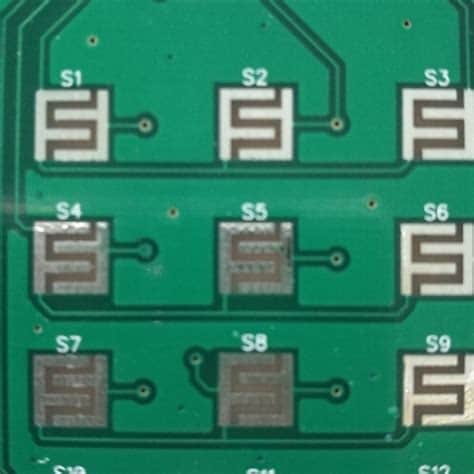
What are Carbon Contacts?
Carbon contacts are a conductive material composed of carbon particles suspended in a polymer binder. When applied to a PCB, they create a conductive pathway that allows electrical signals to pass through the board. Carbon contacts are typically screen-printed onto the PCB surface, forming a thin, durable layer that can withstand harsh environmental conditions and repeated use.
Advantages of Using Carbon Contacts in PCBs
There are several key advantages to using carbon contacts in PCB manufacturing:
- Cost-effective: Carbon contacts are generally less expensive than metal contacts, making them an attractive option for budget-conscious projects.
- Durable: Carbon contacts are highly resistant to wear and tear, making them ideal for applications that require frequent use or exposure to harsh environments.
- Environmentally friendly: Unlike metal contacts, carbon contacts do not require the use of hazardous chemicals or plating processes, making them a more eco-friendly choice.
- Versatile: Carbon contacts can be applied to a wide range of PCB materials, including flexible substrates, making them suitable for a variety of applications.
The Process of Applying Carbon Contacts to PCBs
Step 1: PCB Design and Preparation
Before applying carbon contacts to a PCB, it is essential to ensure that the board is properly designed and prepared. This involves creating a PCB Layout that incorporates the necessary contact points and ensuring that the board surface is clean and free of contaminants.
Step 2: Screen Printing the Carbon Contacts
Once the PCB is prepared, the carbon contacts can be applied using a screen printing process. This involves the following steps:
- Create a stencil: A stencil is created with the desired pattern of the carbon contacts. This stencil is typically made of a fine mesh material that allows the carbon ink to pass through in the desired areas.
- Apply the carbon ink: The carbon ink is then applied to the stencil and spread evenly using a squeegee. The ink passes through the stencil’s openings and onto the PCB surface.
- Cure the ink: After the carbon ink is applied, the PCB is placed in an oven to cure the ink. This process helps the ink adhere to the board surface and ensures that it becomes fully conductive.
Step 3: Testing and Quality Control
After the carbon contacts have been applied and cured, it is important to test the PCB to ensure that the contacts are functioning properly. This typically involves using a Multimeter or other testing equipment to verify that the contacts have the desired electrical properties and that there are no shorts or opens in the circuit.

Best Practices for Incorporating Carbon Contacts into PCB Designs
When designing a PCB that will use carbon contacts, there are several best practices to keep in mind:
- Choose the right carbon ink: Select a carbon ink that is compatible with your PCB material and has the desired electrical properties for your application.
- Design for manufacturability: Ensure that your PCB layout is designed with the screen printing process in mind, with adequate spacing between contacts and other components.
- Consider the curing process: Be aware of the curing requirements for your chosen carbon ink and ensure that your manufacturing process can accommodate these requirements.
- Plan for testing: Incorporate testing points into your PCB design to facilitate quality control and troubleshooting.

Applications of Carbon Contacts in PCBs
Carbon contacts have found use in a wide range of PCB Applications, including:
- Membrane switches: Carbon contacts are commonly used in membrane switches, such as those found in keyboards and Control Panels, due to their durability and low cost.
- Flexible circuits: The versatility of carbon contacts makes them well-suited for use in Flexible PCBs, which can be bent or folded without damaging the contacts.
- Biosensors: Carbon contacts have been used in the development of biosensors, where their biocompatibility and conductivity make them ideal for detecting biological signals.
- Wearable electronics: The durability and flexibility of carbon contacts make them a good choice for use in wearable electronic devices, which must withstand frequent movement and exposure to the elements.

Challenges and Limitations of Carbon Contacts
While carbon contacts offer many benefits, there are also some challenges and limitations to consider:
- Lower conductivity: Carbon contacts typically have a lower conductivity than metal contacts, which can limit their use in high-current applications.
- Limited resolution: The screen printing process used to apply carbon contacts may not be suitable for very fine pitch or high-density designs.
- Compatibility issues: Some carbon inks may not be compatible with certain PCB materials or manufacturing processes, so it is important to carefully select the right ink for your application.
Future Developments in Carbon Contact Technology
As the demand for low-cost, durable, and environmentally friendly PCB solutions continues to grow, researchers and manufacturers are exploring new ways to improve carbon contact technology. Some areas of active research include:
- Nanocarbon materials: The use of nanocarbon materials, such as carbon nanotubes or graphene, could potentially increase the conductivity and performance of carbon contacts.
- Hybrid contacts: Combining carbon contacts with other materials, such as metal nanoparticles, could offer the benefits of both technologies while mitigating their limitations.
- Advanced printing techniques: The development of new printing techniques, such as inkjet printing or aerosol jet printing, could enable the creation of finer and more complex carbon contact patterns.
Frequently Asked Questions (FAQ)
-
Q: Can carbon contacts be used in high-temperature applications?
A: Yes, many carbon inks are designed to withstand high temperatures, making them suitable for use in applications such as automotive electronics or industrial sensors. -
Q: How do the costs of carbon contacts compare to those of metal contacts?
A: Carbon contacts are generally less expensive than metal contacts, as they do not require the use of precious metals or complex plating processes. However, the exact cost savings will depend on the specific application and the chosen carbon ink. -
Q: Are carbon contacts as durable as metal contacts?
A: In many cases, carbon contacts can be more durable than metal contacts, as they are resistant to corrosion, wear, and environmental factors such as humidity and temperature fluctuations. -
Q: Can carbon contacts be used on any type of PCB material?
A: Carbon contacts can be used on a wide range of PCB materials, including FR-4, polyimide, and PET. However, it is important to select a carbon ink that is compatible with your chosen PCB material to ensure optimal performance and adhesion. -
Q: How can I ensure the quality and consistency of carbon contacts in my PCB manufacturing process?
A: To ensure the quality and consistency of carbon contacts, it is important to carefully control the screen printing process, including the selection of the appropriate stencil, ink, and curing conditions. Regular testing and quality control measures, such as electrical continuity and resistance testing, can help identify any issues and maintain consistent performance.
Conclusion
Carbon contacts offer a promising alternative to traditional metal contacts in PCB manufacturing, providing a cost-effective, durable, and environmentally friendly solution for a wide range of applications. By understanding the process of applying carbon contacts to PCBs, as well as the best practices and limitations of this technology, designers and manufacturers can effectively incorporate carbon contacts into their PCB designs and take advantage of their unique benefits. As research and development in this field continue, we can expect to see even more innovative uses of carbon contacts in the future of PCB manufacturing.
| Characteristic | Carbon Contacts | Metal Contacts |
|---|---|---|
| Cost | Lower | Higher |
| Durability | High | Moderate |
| Environmental resistance | High | Moderate |
| Conductivity | Moderate | High |
| Versatility | High | Moderate |
Table 1: Comparison of carbon contacts and metal contacts in PCB manufacturing.
| Application | Benefit of Carbon Contacts |
|---|---|
| Membrane switches | Durability, low cost |
| Flexible circuits | Versatility, durability |
| Biosensors | Biocompatibility, conductivity |
| Wearable electronics | Durability, flexibility |
Table 2: Benefits of carbon contacts in various PCB applications.
No responses yet