What is a PCB Edge Connector?
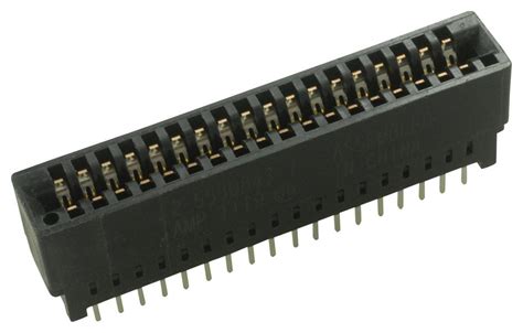
A PCB edge connector is a type of electrical connector that is designed to mate with the edge of a printed circuit board. The edge of the PCB is inserted into a slot in the connector, which establishes an electrical connection between the PCB and the connector. Edge connectors are commonly used in various applications, such as:
- Computer peripherals (e.g., graphics cards, sound cards)
- Industrial control systems
- Automotive electronics
- Telecommunications equipment
Advantages of PCB Edge Connectors
PCB edge connectors offer several advantages over other types of connectors:
- Space-saving design: Edge connectors allow for a compact design, as they do not require additional space on the PCB surface for mounting.
- Cost-effective: Edge connectors are generally less expensive than other types of connectors due to their simple design and manufacturing process.
- High reliability: With proper design and manufacturing, edge connectors can provide a reliable and stable connection.
- Easy installation and removal: PCBs can be easily inserted and removed from edge connectors, facilitating maintenance and upgrades.
The Importance of Edge Connector Bevelling
Edge connector bevelling is the process of creating a smooth, tapered edge on the PCB where it mates with the connector. This process is essential for several reasons:
- Improved contact: Bevelling the edge of the PCB ensures proper contact between the PCB and the connector, reducing the risk of intermittent connections or signal loss.
- Easier insertion: A bevelled edge allows for smoother insertion of the PCB into the connector, reducing the risk of damage to the PCB or connector during the mating process.
- Reduced wear: A properly bevelled edge minimizes wear on the connector contacts, extending the connector’s lifespan.
- Enhanced signal integrity: A well-designed bevel can help maintain signal integrity by reducing impedance discontinuities at the PCB-connector interface.

Edge Connector Bevelling Techniques
There are several techniques used for edge connector bevelling, each with its advantages and disadvantages.
Mechanical Bevelling
Mechanical bevelling involves using abrasive tools, such as sandpaper or files, to manually create the desired bevel on the PCB edge. This method is suitable for low-volume production or prototype development, as it is relatively inexpensive and does not require specialized equipment. However, mechanical bevelling is time-consuming and may result in inconsistencies between boards.
Chemical Bevelling
Chemical bevelling, also known as etching, uses a chemical solution to remove material from the PCB edge, creating the desired bevel. This method is more consistent than mechanical bevelling and is suitable for high-volume production. The chemical composition and exposure time must be carefully controlled to achieve the desired bevel profile without damaging the PCB.
Laser Bevelling
Laser bevelling uses a high-power laser to remove material from the PCB edge, creating a precise and consistent bevel. This method offers several advantages:
- High precision: Laser bevelling can achieve very precise bevel profiles, ensuring optimal contact between the PCB and connector.
- Consistency: Laser bevelling produces consistent results across multiple boards, reducing the risk of connection issues caused by inconsistent bevels.
- High speed: Laser bevelling is a fast process, making it suitable for high-volume production.
- Minimal material removal: Laser bevelling removes only the necessary amount of material, minimizing the risk of damaging the PCB or its components.
However, laser bevelling equipment is more expensive than other bevelling methods, and the process requires skilled operators to ensure optimal results.
Bevelling Process Comparison
| Method | Precision | Consistency | Speed | Cost | Suitable for |
|---|---|---|---|---|---|
| Mechanical | Low | Low | Low | Low | Low-volume, prototypes |
| Chemical | Medium | High | Medium | Medium | High-volume |
| Laser | High | High | High | High | High-volume, high-precision |

Designing for Edge Connector Bevelling
When designing a PCB that will use an edge connector, several factors must be considered to ensure optimal performance and reliability:
- Connector selection: Choose an edge connector that is compatible with the PCB Thickness, copper weight, and required number of contacts.
- Contact pitch: Ensure that the contact pitch of the connector matches the contact spacing on the PCB.
- Bevel angle: Select a bevel angle that is compatible with the connector and provides optimal contact pressure. Common bevel angles range from 20° to 45°.
- Bevel length: Determine the appropriate bevel length based on the connector design and PCB thickness. A longer bevel may be necessary for thicker PCBs to ensure proper contact.
- Copper plating: Ensure that the edge connector contacts are plated with a suitable material, such as gold or palladium-nickel, to provide reliable contact and prevent oxidation.
- Solder Mask: Apply solder mask to the bevelled edge to prevent solder bridging between contacts during the assembly process.
By carefully considering these factors during the design phase, you can ensure that your PCB and edge connector will function reliably and meet the requirements of your application.

Frequently Asked Questions
1. What is the purpose of edge connector bevelling?
Edge connector bevelling creates a smooth, tapered edge on the PCB where it mates with the connector. This process improves contact, eases insertion, reduces wear, and enhances signal integrity.
2. What are the common techniques used for edge connector bevelling?
The common techniques used for edge connector bevelling are mechanical bevelling (using abrasive tools), chemical bevelling (etching), and laser bevelling.
3. Which edge connector bevelling method is best for high-volume production?
Laser bevelling is the most suitable method for high-volume production, as it offers high precision, consistency, and speed. Chemical bevelling is also suitable for high-volume production but may not achieve the same level of precision as laser bevelling.
4. How does the bevel angle affect the PCB-connector interface?
The bevel angle affects the contact pressure between the PCB and the connector. A well-chosen bevel angle ensures optimal contact pressure, which is essential for reliable electrical connection and signal integrity.
5. What should be considered when designing a PCB for use with an edge connector?
When designing a PCB for use with an edge connector, consider factors such as connector selection, contact pitch, bevel angle, bevel length, copper plating, and solder mask application. Careful consideration of these factors ensures optimal performance and reliability of the PCB-connector interface.
In conclusion, edge connector bevelling is a critical process in the manufacturing of PCBs that use edge connectors. By creating a smooth, tapered edge on the PCB, bevelling ensures proper contact, easier insertion, reduced wear, and enhanced signal integrity. Designers must carefully consider various factors when designing PCBs for use with edge connectors, and manufacturers must choose the appropriate bevelling technique based on production volume, precision requirements, and cost considerations. With a well-designed and properly bevelLED PCB edge, your application can achieve reliable and stable electrical connections, ensuring optimal performance and longevity.
No responses yet