Understanding PCB Designators and Overlays
When designing a printed circuit board (PCB), designers often encounter a common issue where designators appear overlaid on extra designators. This can lead to confusion and potentially cause errors during the manufacturing process. In this article, we will explore the reasons behind this phenomenon and provide solutions to avoid designator overlays in your PCB designs.
What are PCB Designators?
PCB designators, also known as reference designators or component designators, are alphanumeric codes used to uniquely identify each component on a PCB. These designators typically consist of a letter prefix followed by a number, such as R1 for a resistor, C2 for a capacitor, or U3 for an integrated circuit.
Designators serve several important purposes:
- They help designers, manufacturers, and assemblers locate and identify specific components on the PCB.
- They facilitate communication between team members during the design and manufacturing process.
- They aid in creating accurate bills of materials (BOM) and assembly instructions.
Why Do Designators Overlay on Extra Designators?
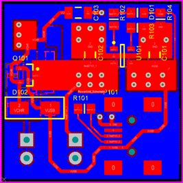
Designator overlays occur when multiple designators are placed too close to each other or when extra designators are generated unintentionally. There are several reasons why this issue may arise:
-
Improper Component Placement: If components are placed too close together on the PCB layout, their designators may overlap, making them difficult to read.
-
Incorrect Designator Settings: Most PCB design software allows users to configure designator settings, such as font size, style, and placement. If these settings are not properly adjusted, designators may overlap or appear in undesired locations.
-
Duplicate Designators: Sometimes, designers may accidentally assign the same designator to multiple components, resulting in duplicate designators that overlap.
-
Automatic Designator Generation: Some PCB design tools have features that automatically generate designators based on component types. If not configured correctly, this can lead to overlapping designators.
Techniques to Avoid Designator Overlays
To prevent designator overlays and ensure a clean, readable PCB design, consider implementing the following techniques:
1. Proper Component Placement
When placing components on your PCB layout, ensure that there is sufficient space between them to accommodate their respective designators. Follow these guidelines:
- Maintain a minimum clearance of 0.5mm between components and their designators.
- Arrange components in a logical and organized manner, grouping similar components together.
- Consider the orientation of components to minimize designator overlaps.
| Component Type | Recommended Spacing |
|---|---|
| Resistors | 0.5mm |
| Capacitors | 0.5mm |
| Integrated Circuits | 1.0mm |
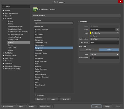
2. Adjusting Designator Settings
Most PCB design software provides options to customize designator settings. Take advantage of these features to optimize designator placement and avoid overlays:
-
Font Size: Choose a font size that is legible but not too large. A font size between 0.8mm and 1.2mm is generally suitable for most PCB designs.
-
Font Style: Select a font style that is clear and easy to read. Sans-serif fonts like Arial or Helvetica are popular choices.
-
Designator Placement: Experiment with different designator placement options, such as above, below, or to the side of the component. Find the placement that minimizes overlaps and improves readability.
| Setting | Recommended Value |
|---|---|
| Font Size | 0.8mm – 1.2mm |
| Font Style | Sans-serif (Arial, Helvetica) |
| Placement | Above, below, or to the side of the component |
3. Manually Adjusting Designator Positions
In some cases, automatic designator placement may not yield the desired results. In such situations, you can manually adjust the position of individual designators:
- Select the designator you want to move in your PCB design software.
- Use the move tool or arrow keys to reposition the designator to a more suitable location.
- Ensure that the designator remains associated with the correct component.
4. Resolving Duplicate Designators
If you encounter duplicate designators in your PCB design, follow these steps to resolve the issue:
- Use the “Find and Replace” or “Rename” feature in your PCB design software to locate duplicate designators.
- Assign unique designators to each component, following a consistent naming convention (e.g., R1, R2, R3 for resistors).
- Double-check the updated designators to ensure they are correct and free of overlaps.
5. Configuring Automatic Designator Generation
If your PCB design software offers automatic designator generation, make sure to configure it properly to avoid overlaps:
- Review the settings for automatic designator generation, such as prefix, numbering, and placement rules.
- Set appropriate constraints to ensure designators are placed in suitable locations and do not overlap with other elements.
- Test the automatic designator generation on a small portion of your design to verify its effectiveness.
FAQ
-
Q: What should I do if I encounter overlapping designators in my PCB design?
A: First, try adjusting the designator settings, such as font size and placement. If that doesn’t resolve the issue, manually reposition the overlapping designators to a more suitable location. -
Q: How can I prevent duplicate designators in my PCB design?
A: Establish a consistent naming convention for your designators and double-check your design for any duplicates. Use the “Find and Replace” or “Rename” feature in your PCB design software to locate and resolve duplicate designators. -
Q: What is the recommended font size for PCB designators?
A: A font size between 0.8mm and 1.2mm is generally suitable for most PCB designs. This ensures that the designators are legible without being too large. -
Q: Can I change the placement of designators in my PCB design software?
A: Yes, most PCB design software allows you to customize designator placement. Experiment with different options, such as above, below, or to the side of the component, to find the placement that minimizes overlaps and improves readability. -
Q: How can I ensure proper spacing between components to avoid designator overlays?
A: Maintain a minimum clearance of 0.5mm between components and their designators. For larger components like integrated circuits, consider increasing the spacing to 1.0mm. Arrange components in a logical and organized manner to minimize overlaps.

Conclusion
Designator overlays on extra designators can be a frustrating issue when designing PCBs. By understanding the causes and implementing the techniques discussed in this article, you can effectively avoid designator overlays and create clean, readable PCB designs.
Remember to:
– Place components with sufficient spacing
– Adjust designator settings for optimal placement and legibility
– Manually reposition designators when necessary
– Resolve duplicate designators using a consistent naming convention
– Configure automatic designator generation settings properly
By following these guidelines, you can streamline your PCB design process, improve communication among team members, and ensure accurate manufacturing and assembly of your PCBs.
No responses yet