Introduction to PCB-Editing
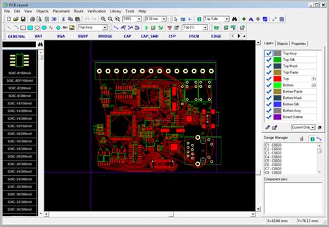
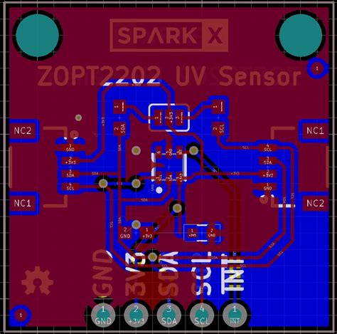
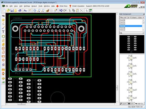
Printed Circuit Board (PCB) design is a crucial aspect of electronic product development. PCB-editing involves making changes to various design objects such as components, traces, vias, and polygons to optimize the layout and functionality of the board. Efficient editing of multiple PCB design objects is essential for streamlining the design process and ensuring the final product meets the desired specifications.
In this article, we will explore the techniques and best practices for editing multiple PCB design objects effectively. We will cover topics such as selection methods, group editing, using shortcuts, and utilizing advanced tools provided by PCB design software. By mastering these techniques, you can significantly improve your productivity and create high-quality PCB designs.
Selecting Multiple Objects for PCB-Editing
The first step in editing multiple PCB design objects is to select them efficiently. Most PCB design software offers various selection methods to help you quickly select the desired objects. Here are some common selection techniques:
1. Click and Drag Selection
The click and drag method allows you to select multiple objects by clicking and dragging your mouse cursor over the desired area. This method is useful when you need to select objects that are in close proximity to each other.
2. Shift + Click Selection
By holding down the Shift key and clicking on individual objects, you can add them to the current selection. This method is helpful when you want to select specific objects that are not necessarily adjacent to each other.
3. Selection by Properties
PCB design software often provides options to select objects based on their properties, such as component type, net name, or layer. This feature is particularly useful when you need to select all objects that share a common property.
For example, you can select all components of a specific type (e.g., resistors) by using the “Select by Component Type” option in your PCB design software.
4. Using Selection Filters
Selection filters allow you to define criteria for selecting objects automatically. You can create filters based on various properties, such as object type, size, or location. This method is beneficial when dealing with complex designs that contain a large number of objects.
| Selection Method | Description | Use Case |
|---|---|---|
| Click and Drag | Select objects by dragging the mouse cursor over an area | Selecting objects in close proximity |
| Shift + Click | Add individual objects to the current selection by holding Shift and clicking | Selecting specific objects not adjacent to each other |
| Selection by Properties | Select objects based on shared properties (e.g., component type, net name) | Selecting all objects with a common property |
| Selection Filters | Define criteria to automatically select objects based on properties, size, or location | Dealing with complex designs with numerous objects |

Group Editing Techniques
Once you have selected the desired objects, you can perform various editing operations on them simultaneously. Group editing techniques allow you to modify multiple objects efficiently, saving time and effort. Here are some common group editing techniques:
1. Move and Rotate
You can move and rotate multiple selected objects at once by using the move and rotate tools in your PCB design software. This technique is useful when you need to reposition or orient a group of objects while maintaining their relative positions.
2. Copy and Paste
Copying and pasting selected objects is a quick way to duplicate them within the same design or across different designs. This technique is handy when you need to create multiple instances of a group of objects or reuse a portion of a design in another project.
3. Modify Properties
Group editing allows you to change the properties of multiple selected objects simultaneously. For example, you can change the color, layer, or net assignment of a group of objects in a single operation. This technique ensures consistency and saves time when making bulk changes to object properties.
4. Align and Distribute
Aligning and distributing selected objects helps in creating a neat and organized PCB layout. Most PCB design software provides tools to align objects horizontally, vertically, or along a specific reference point. You can also distribute objects evenly based on their spacing or center points.
| Group Editing Technique | Description | Use Case |
|---|---|---|
| Move and Rotate | Reposition and orient multiple objects simultaneously | Modifying the placement of a group of objects |
| Copy and Paste | Duplicate selected objects within the same design or across different designs | Creating multiple instances of a group of objects or reusing a portion of a design |
| Modify Properties | Change properties (e.g., color, layer, net assignment) of multiple objects simultaneously | Making bulk changes to object properties for consistency |
| Align and Distribute | Align objects horizontally, vertically, or along a reference point; distribute objects evenly based on spacing or center points | Creating a neat and organized PCB layout |

Using Shortcuts for Efficient PCB-Editing
Keyboard shortcuts can significantly speed up your PCB-editing workflow by reducing the need to navigate through menus and toolbars. Most PCB design software provides a set of default shortcuts for common actions, and many allow you to customize shortcuts according to your preferences. Here are some examples of useful shortcuts:
- Ctrl + C: Copy selected objects
- Ctrl + V: Paste copied objects
- Ctrl + Z: Undo the last action
- Ctrl + Y: Redo the last undone action
- Ctrl + A: Select all objects
- Ctrl + D: Deselect all objects
- Ctrl + M: Move selected objects
- Ctrl + R: Rotate selected objects
To make the most of shortcuts, take the time to learn and memorize the ones you use frequently. You can also print out a cheat sheet or reference guide to keep nearby while working on your PCB designs.

Advanced PCB-Editing Tools
Modern PCB design software offers advanced tools that can greatly enhance your editing capabilities. These tools automate complex tasks and provide intelligent solutions to common design challenges. Some examples of advanced PCB-editing tools include:
1. Auto-Router
An auto-router is a tool that automatically routes traces between components based on predefined rules and constraints. While auto-routers can save time, it is essential to review and manually fine-tune the generated routes to ensure optimal performance and manufacturability.
2. Design Rule Check (DRC)
DRC tools analyze your PCB design for potential errors and violations of design rules. These rules can include minimum clearance distances, trace widths, and drill sizes. Running DRC regularly during the editing process helps catch and resolve issues early, preventing costly mistakes later in the development cycle.
3. 3D Visualization
Many PCB design software packages offer 3D visualization tools that allow you to view your design in a realistic three-dimensional representation. This feature is valuable for checking component clearances, identifying potential mechanical interferences, and communicating the design to stakeholders.
4. Scripting and Automation
Some PCB design software supports scripting languages that allow you to automate repetitive tasks and create custom tools. Scripting can be particularly useful when working on large, complex designs or when you need to perform batch operations on multiple objects.
Best Practices for PCB-Editing
To ensure an efficient and effective PCB-editing process, consider the following best practices:
-
Establish a consistent naming convention for components, nets, and layers to make it easier to navigate and select objects in your design.
-
Use a grid system and snap-to-grid feature to maintain a clean and organized layout. This practice also helps in aligning objects accurately.
-
Create and maintain a library of frequently used components, footprints, and symbols to save time and ensure consistency across designs.
-
Regularly run Design Rule Checks (DRC) to catch and resolve potential issues early in the design process.
-
Use version control systems to track changes, collaborate with team members, and revert to previous versions if needed.
-
Document your design decisions, constraints, and guidelines to facilitate future modifications and maintain design integrity.
Frequently Asked Questions (FAQ)
-
Q: What is the best way to select multiple objects in a PCB design?
A: The best way to select multiple objects depends on the situation. For objects in close proximity, click and drag selection is often the most efficient. For specific objects not adjacent to each other, Shift + Click selection is suitable. When selecting objects based on shared properties or in complex designs, selection by properties or using selection filters can be more effective. -
Q: How can I move multiple objects while maintaining their relative positions?
A: To move multiple objects while maintaining their relative positions, select the objects using one of the selection methods, then use the move tool in your PCB design software. The selected objects will move together as a group, preserving their relative positions. -
Q: Can I change the properties of multiple objects at once?
A: Yes, most PCB design software allows you to modify the properties of multiple selected objects simultaneously. This feature is called group editing and is useful for making bulk changes to object properties, such as color, layer, or net assignment. -
Q: How can I ensure my PCB design is error-free?
A: To ensure your PCB design is error-free, regularly run Design Rule Checks (DRC) using the tools provided by your PCB design software. DRC tools analyze your design for potential errors and violations of design rules, helping you catch and resolve issues early in the development process. -
Q: What are some best practices for efficient PCB-editing?
A: Some best practices for efficient PCB-editing include establishing a consistent naming convention, using a grid system and snap-to-grid feature, creating a library of frequently used components, regularly running DRC, using version control systems, and documenting your design decisions and guidelines.
Conclusion
Editing multiple PCB design objects efficiently is a critical skill for creating high-quality, error-free PCB layouts. By mastering selection methods, group editing techniques, and utilizing advanced tools provided by PCB design software, you can streamline your workflow and improve your productivity.
Remember to establish and follow best practices, such as maintaining a consistent naming convention, using a grid system, and regularly running Design Rule Checks. These practices will help you create clean, organized, and error-free PCB designs.
As you continue to work on PCB designs, keep exploring new tools and techniques to further optimize your editing process. Stay updated with the latest advancements in PCB design software and engage with the PCB design community to learn from others’ experiences and share your own insights.
By mastering the art of editing multiple PCB design objects, you will be well-equipped to tackle complex design challenges and create high-quality PCBs that meet the ever-evolving demands of the electronics industry.

No responses yet