Introduction to PCB-Assembly
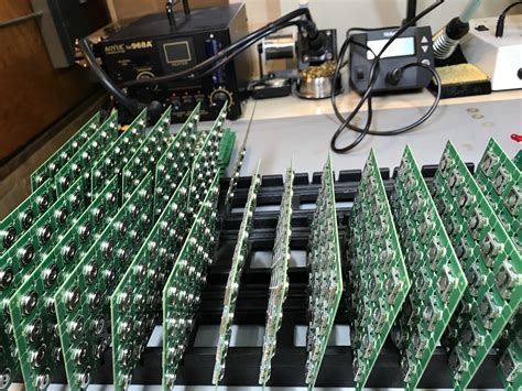
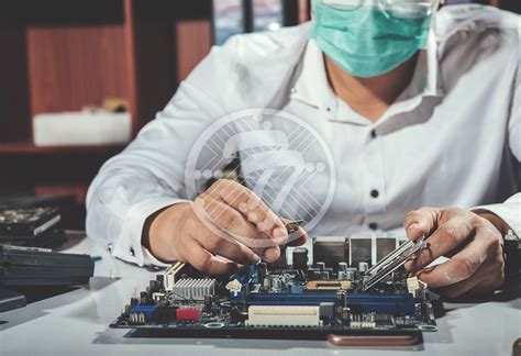
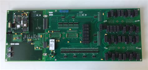
PCB-Assembly, or Printed Circuit Board Assembly, is the process of assembling various electronic components onto a printed circuit board to create a functional electronic device. In the case of multi-board assembly, multiple PCBs are interconnected to form a more complex system. This process involves several steps, including component placement, soldering, and testing, to ensure the proper functioning of the final product.
Key Components in PCB-Assembly
- Printed Circuit Board (PCB)
- Substrate
- Copper traces
- Solder mask
-
Silkscreen
-
Electronic Components
- Resistors
- Capacitors
- Inductors
- Integrated Circuits (ICs)
- Connectors
- Switches
-
LEDs
-
Solder
- Leaded
- Lead-free
PCB-Assembly Methods
There are two primary methods for PCB-Assembly:
- Through-Hole Assembly (THA)
- Components have long leads that are inserted through holes in the PCB
- Leads are soldered to the opposite side of the board
-
Suitable for larger components and high-power applications
-
Surface Mount Assembly (SMA)
- Components have small leads or pads that are soldered directly onto the surface of the PCB
- Allows for higher component density and smaller board sizes
- Requires precise placement and soldering techniques
PCB-Assembly Process
Step 1: Design and Fabrication
- Schematic Design
- Create a schematic diagram of the electronic circuit
-
Specify component values and connections
-
PCB Layout
- Translate the schematic into a physical layout
- Determine component placement and routing of copper traces
-
Consider signal integrity, power distribution, and thermal management
-
Fabrication
- Generate Gerber files and drill files
- Send files to a PCB manufacturer for fabrication
Step 2: Component Preparation
- Procurement
- Purchase components according to the bill of materials (BOM)
-
Ensure components meet specifications and are available in sufficient quantities
-
Inspection
- Visually inspect components for damage or defects
-
Perform electrical tests if necessary
-
Kitting
- Organize components into kits for each PCB
- Label and package kits for assembly
Step 3: PCB-Assembly
- Solder Paste Application (for SMA)
- Apply solder paste to PCB pads using a stencil or screen printing process
-
Inspect for proper solder paste coverage and alignment
-
Component Placement
- Place components onto the PCB according to the assembly drawing
-
Use pick-and-place machines for high-volume production or hand placement for prototypes and low-volume runs
-
Soldering
- Reflow soldering (for SMA)
- Pass the PCB through a reflow oven to melt the solder paste and form solder joints
- Control temperature profile to ensure proper solder joint formation
-
Wave soldering (for THA)
- Pass the PCB over a molten solder wave to form solder joints on the bottom side of the board
- Preheat the board and apply flux to improve solder wetting
-
Inspection
- Visually inspect solder joints for defects such as bridging, insufficient solder, or poor wetting
- Use automated optical inspection (AOI) for high-volume production
Step 4: Multi-Board Assembly
- Interconnect PCBs
- Use connectors, cables, or direct board-to-board connections to join multiple PCBs
-
Ensure proper alignment and secure connections
-
Mechanical Assembly
- Install the assembled PCBs into the final product enclosure
- Secure the PCBs using standoffs, screws, or other fasteners
- Consider thermal management and vibration dampening
Step 5: Testing and Quality Control
- Functional Testing
- Power on the assembled device and perform functional tests
-
Verify proper operation of all features and functions
-
Boundary Scan Testing
- Use boundary scan (JTAG) testing to verify interconnections between ICs and PCBs
-
Identify shorts, opens, and other manufacturing defects
-
Environmental Testing
- Subject the assembled device to temperature, humidity, and vibration tests
-
Ensure the device can withstand the expected operating conditions
-
Final Inspection
- Perform a final visual inspection for any damage or defects
- Verify labeling, packaging, and documentation

Advantages of Multi-Board PCB-Assembly
- Modularity
- Allows for the design of complex systems by breaking them down into smaller, more manageable subsystems
-
Facilitates easier troubleshooting and maintenance
-
Flexibility
- Enables the use of different technologies and materials for each PCB
-
Allows for the optimization of each subsystem for its specific function
-
Scalability
- Simplifies the process of upgrading or expanding the system by adding or replacing individual PCBs
-
Reduces the need for complete system redesign when changes are required
-
Cost-effectiveness
- Minimizes the impact of design changes by limiting them to specific PCBs rather than the entire system
- Allows for the reuse of proven PCB designs in multiple products

Challenges in Multi-Board PCB-Assembly
- Signal Integrity
- Ensuring proper signal transmission between PCBs
-
Minimizing crosstalk, reflections, and other signal integrity issues
-
Power Distribution
- Providing stable and sufficient power to all PCBs in the system
-
Managing power sequencing and avoiding ground loops
-
Thermal Management
- Dissipating heat generated by components on multiple PCBs
-
Ensuring proper airflow and thermal interface between PCBs
-
Mechanical Stability
- Designing robust mechanical interfaces between PCBs
-
Minimizing stress on connectors and other mechanical components
-
Testing and Debugging
- Developing comprehensive test strategies for multi-board systems
- Isolating faults to specific PCBs or interconnections

Best Practices for Multi-Board PCB-Assembly
- Standardization
- Use standardized components, connectors, and interfaces whenever possible
-
Minimize the variety of PCB sizes and shapes to simplify assembly and reduce costs
-
Design for Manufacturing (DFM)
- Follow DFM guidelines to ensure the PCBs can be efficiently manufactured and assembled
-
Consider component placement, orientation, and spacing to facilitate automated assembly processes
-
Documentation
- Maintain accurate and up-to-date schematics, PCB layouts, and assembly drawings
-
Provide clear instructions for assembly, testing, and troubleshooting
-
Collaboration
- Foster communication between design, manufacturing, and quality control teams
-
Regularly review and update processes to incorporate lessons learned and best practices
-
Continuous Improvement
- Monitor and analyze assembly yields, defect rates, and customer feedback
- Implement process improvements to increase efficiency, reduce costs, and enhance product quality
Frequently Asked Questions (FAQ)
- What is the difference between through-hole and surface mount assembly?
-
Through-hole assembly involves inserting component leads through holes in the PCB and soldering them on the opposite side. Surface mount assembly involves soldering components directly onto the surface of the PCB. Surface mount assembly allows for higher component density and smaller board sizes, while through-hole assembly is suitable for larger components and high-power applications.
-
What are the key steps in the PCB-assembly process?
-
The key steps in the PCB-assembly process include design and fabrication, component preparation, PCB-assembly (solder paste application, component placement, soldering, and inspection), multi-board assembly (interconnecting PCBs and mechanical assembly), and testing and quality control.
-
What are the advantages of multi-board PCB-assembly?
-
Multi-board PCB-assembly offers several advantages, including modularity (breaking down complex systems into smaller subsystems), flexibility (using different technologies and materials for each PCB), scalability (easily upgrading or expanding the system), and cost-effectiveness (minimizing the impact of design changes and allowing for the reuse of proven PCB designs).
-
What are some of the challenges in multi-board PCB-assembly?
-
Challenges in multi-board PCB-assembly include ensuring signal integrity between PCBs, providing stable and sufficient power distribution, managing thermal dissipation, ensuring mechanical stability, and developing comprehensive testing and debugging strategies.
-
What are some best practices for multi-board PCB-assembly?
- Best practices for multi-board PCB-assembly include standardization (using standardized components and interfaces), design for manufacturing (following DFM guidelines), thorough documentation, collaboration between teams, and continuous improvement through monitoring and analyzing assembly yields, defect rates, and customer feedback.
Conclusion
Multi-board PCB-assembly is a complex process that involves the interconnection of multiple printed circuit boards to create a functional electronic device. By understanding the key components, assembly methods, and process steps involved in multi-board PCB-assembly, designers and manufacturers can work together to create high-quality, reliable, and cost-effective electronic products.
To ensure the success of multi-board PCB-assembly projects, it is essential to follow best practices such as standardization, design for manufacturing, thorough documentation, collaboration, and continuous improvement. By addressing the challenges associated with signal integrity, power distribution, thermal management, mechanical stability, and testing, teams can optimize the performance and reliability of their multi-board assemblies.
As technology continues to advance and electronic devices become increasingly complex, the importance of effective multi-board PCB-assembly will only continue to grow. By staying up-to-date with the latest techniques, tools, and best practices, designers and manufacturers can remain competitive in this rapidly evolving industry and deliver innovative, high-quality products to their customers.

No responses yet