Introduction to Circuit Connectivity
Circuit connectivity is a crucial aspect of electronic design that involves defining the connections between various components in a circuit. Creating accurate and clear circuit connectivity schematics is essential for ensuring proper functionality, manufacturability, and maintainability of electronic devices. In this article, we will delve into the fundamentals of circuit connectivity, explore different types of schematics, and discuss best practices for creating effective circuit diagrams.
Understanding the Basics of Circuit Connectivity
What is Circuit Connectivity?
Circuit connectivity refers to the way in which electronic components are interconnected to form a functional circuit. It involves defining the electrical paths and connections between components such as resistors, capacitors, transistors, and integrated circuits (ICs). The primary goal of circuit connectivity is to ensure that the desired electrical signals flow correctly between the components, enabling the circuit to perform its intended function.
The Importance of Circuit Connectivity Schematics
Circuit connectivity schematics, also known as circuit diagrams or schematic diagrams, are visual representations of the electrical connections in a circuit. These schematics serve several important purposes:
-
Design Communication: Schematics provide a clear and standardized way to communicate the design intent to other engineers, technicians, and stakeholders involved in the project.
-
Documentation: Circuit diagrams act as a permanent record of the circuit design, making it easier to understand, troubleshoot, and modify the circuit in the future.
-
Manufacturing: Schematics are used as a guide during the manufacturing process, helping technicians and assembly line workers correctly place and connect components on a printed circuit board (PCB).
-
Troubleshooting: When issues arise in a circuit, schematics are invaluable for identifying potential problems and tracing signal paths to pinpoint the source of the issue.
Key Elements of Circuit Connectivity Schematics
To create effective circuit connectivity schematics, it is important to understand the key elements that make up these diagrams:
-
Symbols: Schematic symbols are standardized graphical representations of electronic components. Each component has a specific symbol that conveys its function and characteristics.
-
Lines: Lines in a schematic represent the electrical connections between components. Solid lines indicate a direct connection, while dashed lines may represent a logical or indirect connection.
-
Labels: Labels are used to identify components, signal names, and important nodes in the circuit. They provide clarity and make it easier to reference specific parts of the schematic.
-
Ports: Ports are used to represent the inputs and outputs of a circuit or a subsystem. They are typically labeled with signal names and may include additional information such as voltage levels or current ratings.
-
Ground Symbols: Ground symbols indicate a common reference point in the circuit, usually representing a connection to the earth or a low-impedance path to a power supply.

Types of Circuit Connectivity Schematics
There are several types of circuit connectivity schematics, each serving a specific purpose and providing a different level of detail. Let’s explore some of the most common types:
Block Diagrams
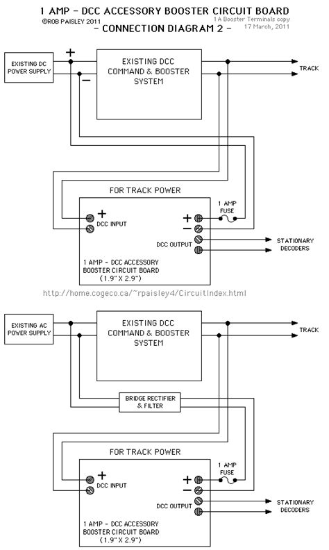
Block diagrams provide a high-level overview of a system or circuit, focusing on the major functional blocks and their interconnections. They are useful for understanding the overall architecture and signal flow without delving into the details of individual components.
Functional Schematics
Functional schematics represent the circuit at a higher level of abstraction, emphasizing the logical functions performed by different sections of the circuit. They often use simplified symbols and omit component-level details, making them easier to understand for non-technical stakeholders.
Detailed Schematics
Detailed schematics, also known as component-level schematics, provide a comprehensive representation of the circuit, including all the individual components and their interconnections. These schematics are essential for circuit analysis, troubleshooting, and manufacturing.
Hierarchical Schematics
Hierarchical schematics are used for complex circuits that can be broken down into smaller, more manageable subsystems. They consist of multiple levels, with each level representing a specific subsystem or functional block. Hierarchical schematics make it easier to navigate and understand large circuits by providing a structured and modular approach.

Best Practices for Creating Circuit Connectivity Schematics
To create clear, accurate, and effective circuit connectivity schematics, consider the following best practices:
-
Use Consistent Symbols: Ensure that you use standardized symbols for components throughout the schematic. Consistency helps avoid confusion and makes it easier for others to interpret the diagram.
-
Organize the Schematic: Arrange the components and connections in a logical and readable manner. Group related components together and minimize the crossing of signal lines to improve clarity.
-
Label Components and Signals: Clearly label all components, signal names, and important nodes in the schematic. Use descriptive names that convey the purpose or function of each element.
-
Follow Naming Conventions: Adhere to established naming conventions for components, signals, and nets. This helps maintain consistency and makes it easier to collaborate with other engineers.
-
Use Appropriate Line Styles: Use solid lines for direct connections and dashed lines for logical or indirect connections. Be consistent with line styles throughout the schematic.
-
Provide Power and Ground Connections: Clearly indicate power and ground connections in the schematic. Use appropriate symbols and labels to differentiate between different power supplies and ground references.
-
Include Relevant Information: Provide additional information such as component values, ratings, and tolerances when necessary. This helps ensure proper component selection and aids in troubleshooting.
-
Maintain Readability: Keep the schematic clean and uncluttered. Avoid overcrowding the diagram and use appropriate spacing between components and connections.
-
Use Hierarchical Approach: For complex circuits, consider using a hierarchical approach to break down the schematic into smaller, more manageable subsystems. This improves overall readability and makes it easier to navigate the schematic.
-
Perform Thorough Review: Always review the schematic for accuracy, completeness, and adherence to design standards. Have colleagues or subject matter experts review the schematic to catch any errors or inconsistencies.

Common Pitfalls to Avoid in Circuit Connectivity Schematics
When creating circuit connectivity schematics, be aware of the following common pitfalls and take steps to avoid them:
-
Incorrect or Inconsistent Symbols: Using incorrect or inconsistent symbols can lead to confusion and misinterpretation of the schematic. Always use standardized symbols and maintain consistency throughout the diagram.
-
Unclear or Ambiguous Labeling: Poor labeling practices, such as using non-descriptive or ambiguous names, can make it difficult to understand the purpose and function of components and signals. Use clear and meaningful labels that convey the necessary information.
-
Incomplete or Missing Connections: Failing to include all the necessary connections or accidentally leaving out components can result in an incomplete or non-functional schematic. Double-check the schematic to ensure all connections are properly represented.
-
Inconsistent Line Styles: Inconsistent use of line styles can lead to confusion and misinterpretation of the schematic. Maintain consistent line styles for direct and indirect connections throughout the diagram.
-
Overcrowding or Poor Organization: An overcrowded or poorly organized schematic can be difficult to read and understand. Ensure proper spacing between components and connections, and arrange the elements in a logical and readable manner.
-
Neglecting Power and Ground Connections: Forgetting to include power and ground connections can lead to an incomplete or non-functional schematic. Always include appropriate symbols and labels for power supplies and ground references.
-
Lack of Documentation: Failing to provide sufficient documentation or annotations in the schematic can make it challenging for others to understand and work with the circuit. Include relevant information and comments to aid in comprehension and troubleshooting.
-
Skipping the Review Process: Not performing a thorough review of the schematic can result in errors and inconsistencies going unnoticed. Always allocate time for a comprehensive review and have others provide feedback and catch any issues.
Tools and Software for Creating Circuit Connectivity Schematics
There are various tools and software available for creating circuit connectivity schematics. Some popular options include:
-
Autodesk Eagle: A widely used PCB design software that offers schematic capture, layout editing, and library management features.
-
KiCad: A free and open-source EDA (Electronic Design Automation) software suite that provides schematic capture, PCB layout, and simulation capabilities.
-
Altium Designer: A comprehensive PCB design software that offers advanced schematic capture, layout editing, and simulation features.
-
OrCAD: A powerful PCB design software that includes schematic capture, simulation, and layout capabilities.
-
Proteus: An integrated EDA software that combines schematic capture, simulation, and PCB layout features.
When selecting a tool or software for creating circuit connectivity schematics, consider factors such as ease of use, compatibility with your design workflow, availability of component libraries, and collaboration features.
Frequently Asked Questions (FAQ)
-
Q: What is the difference between a schematic and a circuit diagram?
A: A schematic and a circuit diagram are essentially the same things. Both terms refer to a visual representation of the electrical connections and components in a circuit. -
Q: How do I choose the right symbols for my schematic?
A: When selecting symbols for your schematic, refer to industry-standard symbol libraries or the documentation provided by the component manufacturers. Consistency is key, so make sure to use the same symbols throughout your schematic. -
Q: Can I use different software tools for schematic capture and PCB layout?
A: Yes, it is possible to use different software tools for schematic capture and PCB layout. However, using an integrated EDA suite that combines both functionalities can streamline your design process and ensure seamless data transfer between the schematic and layout stages. -
Q: How detailed should my schematic be?
A: The level of detail in your schematic depends on its purpose and the intended audience. For a high-level overview, a block diagram or functional schematic may suffice. For manufacturing or troubleshooting purposes, a detailed component-level schematic is necessary. -
Q: What should I do if I find an error in my schematic after the design is complete?
A: If you discover an error in your schematic after the design is complete, it is important to document the issue and communicate it to all relevant stakeholders. Create a revised version of the schematic with the necessary corrections and ensure that the updated schematic is used for any future work on the circuit.
Conclusion
Creating accurate and clear circuit connectivity schematics is a critical skill for any electronics engineer or designer. By understanding the basics of circuit connectivity, following best practices, and utilizing the right tools and software, you can create schematics that effectively communicate your design intent and facilitate the successful realization of your electronic projects.
Remember to use consistent symbols, organize your schematic logically, provide clear labeling, and perform thorough reviews to ensure the quality and accuracy of your circuit diagrams. By avoiding common pitfalls and continuously refining your schematic creation skills, you can enhance the efficiency and reliability of your electronic designs.
As technology advances and circuits become more complex, the importance of well-crafted circuit connectivity schematics will only continue to grow. By mastering this fundamental aspect of electronic design, you can contribute to the development of innovative and reliable electronic systems that shape our world.

No responses yet