What is a PCB Cutout?
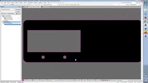
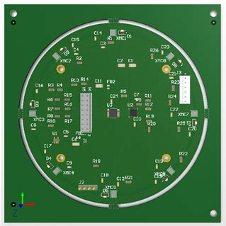
A PCB (Printed Circuit Board) cutout is a unique shape or design cut into the board itself, deviating from the standard rectangular or square shape. These cutouts can serve various purposes, such as accommodating specific components, improving thermal management, or enhancing the overall aesthetics of the board. PCB cutouts are an essential aspect of PCB design, as they allow for greater flexibility and functionality in the final product.
Types of PCB Cutouts
There are several types of PCB cutouts, each serving a specific purpose. Some of the most common types include:
-
Component Cutouts: These cutouts are designed to accommodate specific components that may not fit within the standard board layout. For example, a cutout may be necessary to fit a large connector or a heat sink.
-
Mounting Hole Cutouts: These cutouts are used to create mounting holes for the PCB to be secured to an enclosure or chassis. The size and placement of these cutouts depend on the specific mounting requirements of the project.
-
Thermal Cutouts: These cutouts are designed to improve the thermal management of the PCB by allowing for better airflow or heat dissipation. They are often used in high-power applications or when dealing with components that generate significant amounts of heat.
-
Aesthetic Cutouts: These cutouts are primarily used for aesthetic purposes, such as creating a unique board shape or adding decorative elements to the PCB.
Designing PCB Cutouts
When designing PCB cutouts, several factors must be considered to ensure the best possible results. These factors include:
1. Mechanical Constraints
The mechanical constraints of the project must be taken into account when designing PCB cutouts. This includes considering the size and shape of the enclosure or chassis in which the PCB will be mounted, as well as any specific mounting requirements. The cutouts must be designed to allow for proper fitment and secure mounting of the PCB.
2. Electrical Constraints
The electrical constraints of the project must also be considered when designing PCB cutouts. This includes ensuring that the cutouts do not interfere with the electrical functionality of the board, such as by severing important traces or creating unintended short circuits. It is important to carefully plan the placement of cutouts in relation to the electrical components and traces on the board.
3. Manufacturing Constraints
The manufacturing constraints of the project must be taken into account when designing PCB cutouts. This includes considering the capabilities and limitations of the PCB manufacturing process being used. Some manufacturing processes may have limitations on the minimum size or spacing of cutouts, while others may have specific requirements for the shape or placement of cutouts.
4. Assembly Constraints
The assembly constraints of the project must also be considered when designing PCB cutouts. This includes ensuring that the cutouts do not interfere with the assembly process, such as by making it difficult to place or solder components. It is important to consider the placement of cutouts in relation to the components and connectors on the board, as well as any specific assembly requirements.

Implementing PCB Cutouts
Once the PCB cutouts have been designed, they must be implemented in the PCB layout. This typically involves creating the cutouts in the PCB design software and specifying the appropriate parameters, such as the size, shape, and location of the cutouts.
PCB Design Software
Most modern PCB design software packages include tools for creating and managing PCB cutouts. These tools allow designers to easily create, modify, and place cutouts on the board layout. Some popular PCB design software packages include:
- Altium Designer
- KiCad
- Eagle
- OrCAD
- Cadence Allegro
Cutout Parameters
When implementing PCB cutouts in the design software, several parameters must be specified to ensure the correct creation of the cutouts. These parameters include:
-
Size: The size of the cutout must be specified, typically in terms of width and height or diameter, depending on the shape of the cutout.
-
Shape: The shape of the cutout must be specified, such as rectangular, circular, or a custom shape.
-
Location: The location of the cutout on the board must be specified, typically in terms of X and Y coordinates.
-
Layer: The layer on which the cutout should be created must be specified, such as the top layer, bottom layer, or an inner layer.
Cutout Creation
Once the cutout parameters have been specified in the PCB design software, the cutouts can be created on the board layout. This typically involves using the appropriate tools within the software to draw or place the cutouts on the board.
It is important to ensure that the cutouts are created on the correct layer and in the correct location, as specified in the design. Any errors in the creation of the cutouts can lead to issues with the manufacturing or assembly of the PCB.

Manufacturing PCB Cutouts
Once the PCB layout has been finalized with the cutouts, the board can be sent for manufacturing. The manufacturing process for PCBs with cutouts is similar to that of standard PCBs, with a few additional steps to create the cutouts.
Milling
One common method for creating PCB cutouts is through milling. This involves using a computer-controlled milling machine to remove material from the PCB in the desired shape and size of the cutout. Milling is typically used for larger cutouts or those with more complex shapes.
Routing
Another common method for creating PCB cutouts is through routing. This involves using a computer-controlled router to remove material from the PCB in the desired shape and size of the cutout. Routing is typically used for smaller cutouts or those with simpler shapes.
Punching
For simpler cutouts, such as circular mounting holes, punching may be used instead of milling or routing. This involves using a punch tool to create the cutout in a single step, rather than removing material gradually.

Advantages of PCB Cutouts
PCB cutouts offer several advantages over standard rectangular or square PCBs, including:
-
Improved Functionality: PCB cutouts can be used to accommodate specific components or features that would not fit on a standard board shape, allowing for greater functionality and flexibility in the design.
-
Better Thermal Management: PCB cutouts can be used to improve the thermal management of the board, by allowing for better airflow or heat dissipation. This is particularly important in high-power applications or when dealing with components that generate significant amounts of heat.
-
Enhanced Aesthetics: PCB cutouts can be used to create unique and visually appealing board shapes, which can help to differentiate a product from competitors and improve its overall aesthetics.
-
Reduced Size and Weight: PCB cutouts can be used to reduce the overall size and weight of the board, by removing unnecessary material. This can be particularly important in applications where space and weight are limited, such as in portable devices or aerospace equipment.
Disadvantages of PCB Cutouts
While PCB cutouts offer several advantages, there are also some potential disadvantages to consider, including:
-
Increased Manufacturing Complexity: PCBs with cutouts are generally more complex to manufacture than standard rectangular or square boards, which can increase the overall cost and lead time of the project.
-
Reduced Mechanical Strength: Depending on the size and location of the cutouts, they can potentially reduce the mechanical strength of the board, making it more susceptible to damage or failure.
-
Interference with Electrical Functionality: If not designed properly, PCB cutouts can potentially interfere with the electrical functionality of the board, such as by severing important traces or creating unintended short circuits.
Best Practices for PCB Cutouts
To ensure the best possible results when designing and implementing PCB cutouts, there are several best practices that should be followed, including:
-
Careful Planning: PCB cutouts should be carefully planned and designed, taking into account all of the mechanical, electrical, manufacturing, and assembly constraints of the project.
-
Proper Placement: Cutouts should be placed in locations that do not interfere with the electrical functionality or mechanical strength of the board, and that allow for proper fitment and assembly of the PCB.
-
Adequate Clearance: Adequate clearance should be provided around cutouts to ensure that they do not interfere with nearby components or traces, and to allow for proper manufacturing and assembly.
-
Consistent Design: Cutouts should be designed consistently across the board, with uniform sizes, shapes, and spacing where possible, to simplify the manufacturing and assembly processes.
-
Testing and Verification: The PCB layout should be thoroughly tested and verified before being sent for manufacturing, to ensure that the cutouts are properly designed and placed, and that they do not interfere with the electrical or mechanical functionality of the board.
Frequently Asked Questions (FAQs)
-
What is the purpose of PCB cutouts?
PCB cutouts serve various purposes, such as accommodating specific components, improving thermal management, enhancing aesthetics, or reducing the overall size and weight of the board. -
What are the different types of PCB cutouts?
The different types of PCB cutouts include component cutouts, mounting hole cutouts, thermal cutouts, and aesthetic cutouts. -
What factors should be considered when designing PCB cutouts?
When designing PCB cutouts, factors such as mechanical constraints, electrical constraints, manufacturing constraints, and assembly constraints should be considered. -
How are PCB cutouts manufactured?
PCB cutouts can be manufactured using various methods, such as milling, routing, or punching, depending on the size, shape, and complexity of the cutout. -
What are some best practices for designing and implementing PCB cutouts?
Some best practices for designing and implementing PCB cutouts include careful planning, proper placement, adequate clearance, consistent design, and thorough testing and verification.
Conclusion
PCB cutouts are a valuable tool for designers and engineers, allowing for greater flexibility and functionality in the design of printed circuit boards. By carefully planning and designing cutouts, taking into account all of the relevant constraints and best practices, designers can create PCBs that are optimized for their specific applications and requirements.
While PCB cutouts do come with some potential disadvantages, such as increased manufacturing complexity and reduced mechanical strength, these can be mitigated through proper design and implementation. Ultimately, the benefits of PCB cutouts, including improved functionality, better thermal management, enhanced aesthetics, and reduced size and weight, make them a worthwhile consideration for many PCB design projects.
As PCB technology continues to evolve and advance, it is likely that the use of cutouts will become even more widespread and sophisticated. By staying up-to-date with the latest design tools, manufacturing processes, and best practices, designers and engineers can continue to push the boundaries of what is possible with PCB cutouts and create ever more innovative and effective products.

No responses yet