Understanding the SPI Flash Memory
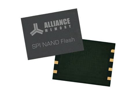
The NanoBoard NB1 is equipped with a SPI flash memory chip, which is a type of non-volatile memory that retains its contents even when power is removed. The specific flash chip used on the NanoBoard NB1 may vary depending on the version and manufacturing date, but it typically has a capacity of several megabytes.
SPI Flash Memory Characteristics
SPI flash memories have several key characteristics that make them suitable for embedded applications:
-
Non-volatile storage: The contents of the flash memory are retained even when power is removed, making it ideal for storing firmware, configuration data, and user settings.
-
High-speed interface: SPI flash memories communicate using the Serial Peripheral Interface (SPI) protocol, which allows for fast data transfer rates.
-
Erase and write operations: Flash memories can be erased and written in blocks or pages, allowing for efficient data modification.
-
Wear leveling: Modern SPI flash chips often include wear leveling mechanisms to distribute erase and write operations evenly across the memory cells, extending the lifespan of the device.
SPI Flash Memory Organization
SPI flash memories are organized into blocks, pages, and sectors. Understanding this organization is essential for efficient data storage and retrieval.
| Unit | Description |
|---|---|
| Block | The largest erasable unit in a flash memory, typically ranging from 4KB to 256KB. |
| Page | The smallest writable unit in a flash memory, usually ranging from 256 bytes to 4KB. |
| Sector | A group of pages that can be erased together, often used for file system management. |
It’s important to consider the erase and write granularity when working with SPI flash memories to ensure optimal performance and minimize wear on the memory cells.
Interfacing with the SPI Flash Memory
To access the SPI flash memory on the NanoBoard NB1, you need to establish a communication interface between the microcontroller and the flash chip. This involves configuring the SPI peripheral, connecting the appropriate pins, and implementing the necessary software drivers.
Hardware Connections
The NanoBoard NB1 provides dedicated SPI pins for interfacing with the flash memory. These pins typically include:
- MOSI (Master Out Slave In): Transmits data from the microcontroller to the flash chip.
- MISO (Master In Slave Out): Receives data from the flash chip to the microcontroller.
- SCK (Serial Clock): Provides the clock signal for synchronizing data transfer.
- CS (Chip Select): Enables or disables the flash chip for communication.
Consult the NanoBoard NB1 documentation or schematic to identify the specific pins used for the SPI flash interface.
Configuring the SPI Peripheral
To communicate with the SPI flash memory, you need to configure the microcontroller’s SPI peripheral. This involves setting the appropriate clock speed, data mode, and other parameters. The exact configuration steps may vary depending on the microcontroller and the software development environment you are using.
Here’s an example of configuring the SPI peripheral using the STM32 HAL library:
void spi_init(void)
{
    hspi.Instance = SPI1;
    hspi.Init.Mode = SPI_MODE_MASTER;
    hspi.Init.Direction = SPI_DIRECTION_2LINES;
    hspi.Init.DataSize = SPI_DATASIZE_8BIT;
    hspi.Init.CLKPolarity = SPI_POLARITY_LOW;
    hspi.Init.CLKPhase = SPI_PHASE_1EDGE;
    hspi.Init.NSS = SPI_NSS_SOFT;
    hspi.Init.BaudRatePrescaler = SPI_BAUDRATEPRESCALER_4;
    hspi.Init.FirstBit = SPI_FIRSTBIT_MSB;
    hspi.Init.TIMode = SPI_TIMODE_DISABLE;
    hspi.Init.CRCCalculation = SPI_CRCCALCULATION_DISABLE;
    hspi.Init.CRCPolynomial = 7;
    if (HAL_SPI_Init(&hspi) != HAL_OK)
    {
        Error_Handler();
    }
}
This code snippet initializes the SPI1 peripheral with the desired configuration, such as master mode, 8-bit data size, and a specific baud rate prescaler.
Implementing Software Drivers
To interact with the SPI flash memory, you need to implement software drivers that handle the low-level communication protocols. These drivers typically include functions for sending commands, reading status registers, and transferring data.
Here’s an example of a simple function to read the status register of the SPI flash chip:
uint8_t spi_flash_read_status(void)
{
    uint8_t status;
    uint8_t command = 0x05; // Read status register command

    HAL_GPIO_WritePin(CS_GPIO_Port, CS_Pin, GPIO_PIN_RESET);
    HAL_SPI_Transmit(&hspi, &command, 1, HAL_MAX_DELAY);
    HAL_SPI_Receive(&hspi, &status, 1, HAL_MAX_DELAY);
    HAL_GPIO_WritePin(CS_GPIO_Port, CS_Pin, GPIO_PIN_SET);

    return status;
}
This function sends the read status register command (0x05) to the SPI flash chip, reads the status byte, and returns it to the caller.
You’ll need to implement additional functions for erasing, writing, and reading data from the flash memory based on the specific commands and protocols supported by your flash chip.

Reading and Writing Data
Once you have established the communication interface and implemented the necessary software drivers, you can start reading and writing data to the SPI flash memory.
Erasing Flash Memory
Before writing new data to the flash memory, you may need to erase the target blocks or sectors. Erasing sets all the bits in the specified region to 1.
Here’s an example of a function to erase a sector in the SPI flash memory:
void spi_flash_erase_sector(uint32_t sector_address)
{
    uint8_t command[4];
    command[0] = 0x20; // Sector erase command
    command[1] = (sector_address >> 16) & 0xFF;
    command[2] = (sector_address >> 8) & 0xFF;
    command[3] = sector_address & 0xFF;

    spi_flash_write_enable();
    HAL_GPIO_WritePin(CS_GPIO_Port, CS_Pin, GPIO_PIN_RESET);
    HAL_SPI_Transmit(&hspi, command, 4, HAL_MAX_DELAY);
    HAL_GPIO_WritePin(CS_GPIO_Port, CS_Pin, GPIO_PIN_SET);
    spi_flash_wait_busy();
}
This function sends the sector erase command (0x20) along with the sector address to the SPI flash chip. It also enables writing, asserts the chip select pin, and waits for the erase operation to complete.
Writing Data
To write data to the SPI flash memory, you typically use the page program command. This allows you to write one or more pages of data at a time.
Here’s an example of a function to write data to a page in the SPI flash memory:
void spi_flash_write_page(uint32_t page_address, uint8_t *data, uint16_t size)
{
    uint8_t command[4];
    command[0] = 0x02; // Page program command
    command[1] = (page_address >> 16) & 0xFF;
    command[2] = (page_address >> 8) & 0xFF;
    command[3] = page_address & 0xFF;

    spi_flash_write_enable();
    HAL_GPIO_WritePin(CS_GPIO_Port, CS_Pin, GPIO_PIN_RESET);
    HAL_SPI_Transmit(&hspi, command, 4, HAL_MAX_DELAY);
    HAL_SPI_Transmit(&hspi, data, size, HAL_MAX_DELAY);
    HAL_GPIO_WritePin(CS_GPIO_Port, CS_Pin, GPIO_PIN_SET);
    spi_flash_wait_busy();
}
This function sends the page program command (0x02) along with the page address and the data to be written. It enables writing, asserts the chip select pin, transfers the data, and waits for the write operation to complete.
Reading Data
Reading data from the SPI flash memory is straightforward using the read data command. You can specify the starting address and the number of bytes to read.
Here’s an example of a function to read data from the SPI flash memory:
void spi_flash_read_data(uint32_t address, uint8_t *data, uint16_t size)
{
    uint8_t command[4];
    command[0] = 0x03; // Read data command
    command[1] = (address >> 16) & 0xFF;
    command[2] = (address >> 8) & 0xFF;
    command[3] = address & 0xFF;

    HAL_GPIO_WritePin(CS_GPIO_Port, CS_Pin, GPIO_PIN_RESET);
    HAL_SPI_Transmit(&hspi, command, 4, HAL_MAX_DELAY);
    HAL_SPI_Receive(&hspi, data, size, HAL_MAX_DELAY);
    HAL_GPIO_WritePin(CS_GPIO_Port, CS_Pin, GPIO_PIN_SET);
}
This function sends the read data command (0x03) along with the starting address, asserts the chip select pin, and receives the specified number of bytes into the provided buffer.

Implementing a File System
While the SPI flash memory provides raw storage, it’s often beneficial to implement a file system on top of it to organize and manage data more effectively. A file system abstracts the low-level details of the flash memory and provides a structured way to store and retrieve files.
Choosing a File System
There are several file systems suitable for embedded systems, each with its own characteristics and trade-offs. Some popular options include:
-
FatFs: A generic FAT file system module for small embedded systems, widely used due to its simplicity and compatibility.
-
LittleFS: A lightweight file system designed for flash-based storage in resource-constrained environments, offering wear leveling and power-loss resilience.
-
SPIFFS: A file system optimized for SPI NOR flash devices, providing a simple and efficient way to store and retrieve files.
Consider factors such as memory footprint, performance, and feature set when selecting a file system for your project.
Porting a File System
Once you have chosen a file system, you need to port it to work with the SPI flash memory on the NanoBoard NB1. This involves implementing the low-level disk I/O functions that interface with your flash memory drivers.
Here’s an example of porting the FatFs file system to work with the SPI flash memory:
#include "ff.h"
#include "diskio.h"

DSTATUS disk_initialize(BYTE pdrv)
{
    // Initialize the SPI flash memory
    spi_flash_init();
    return RES_OK;
}

DSTATUS disk_status(BYTE pdrv)
{
    // Check the status of the SPI flash memory
    // Return the appropriate status code
    return RES_OK;
}

DRESULT disk_read(BYTE pdrv, BYTE *buff, DWORD sector, UINT count)
{
    // Read data from the SPI flash memory
    for (UINT i = 0; i < count; i++)
    {
        spi_flash_read_data(sector * _MAX_SS, buff, _MAX_SS);
        sector++;
        buff += _MAX_SS;
    }
    return RES_OK;
}

DRESULT disk_write(BYTE pdrv, const BYTE *buff, DWORD sector, UINT count)
{
    // Write data to the SPI flash memory
    for (UINT i = 0; i < count; i++)
    {
        spi_flash_erase_sector(sector * _MAX_SS);
        spi_flash_write_page(sector * _MAX_SS, buff, _MAX_SS);
        sector++;
        buff += _MAX_SS;
    }
    return RES_OK;
}

DRESULT disk_ioctl(BYTE pdrv, BYTE cmd, void *buff)
{
    // Perform miscellaneous functions
    // Handle the appropriate IOCTL commands
    return RES_OK;
}
These functions map the file system’s disk I/O operations to the corresponding SPI flash memory operations, such as initializing the flash, reading data, writing data, and performing control functions.
Using the File System
With the file system ported and initialized, you can use the standard file system APIs to create, read, write, and delete files on the SPI flash memory.
Here’s an example of creating a file and writing data to it:
FATFS fs;
FIL file;
UINT bytesWritten;

f_mount(&fs, "", 0);
f_open(&file, "data.txt", FA_WRITE | FA_CREATE_ALWAYS);
f_write(&file, "Hello, World!", 13, &bytesWritten);
f_close(&file);
f_mount(NULL, "", 0);
This code mounts the file system, creates a file named “data.txt”, writes the string “Hello, World!” to the file, closes the file, and unmounts the file system.
Similarly, you can use other file system functions to read files, list directories, and perform various file operations on the SPI flash memory.

Frequently Asked Questions (FAQ)
-
Q: What is the storage capacity of the SPI flash memory on the NanoBoard NB1?
A: The storage capacity of the SPI flash memory on the NanoBoard NB1 can vary depending on the specific version and configuration. Typically, it ranges from a few megabytes to several tens of megabytes. Consult the documentation or specifications of your particular NanoBoard NB1 to determine the exact capacity. -
Q: Can I use the SPI flash memory for storing firmware updates?
A: Yes, the SPI flash memory on the NanoBoard NB1 is well-suited for storing firmware updates. You can allocate a dedicated region of the flash memory for storing firmware images and implement a bootloader that can load and execute the firmware from the flash memory. -
Q: Is it possible to access the SPI flash memory from multiple threads or tasks simultaneously?
A: Access to the SPI flash memory should be synchronized and mutually exclusive to prevent data corruption. If you have multiple threads or tasks that need to access the flash memory, you should implement proper synchronization mechanisms, such as mutexes or semaphores, to ensure that only one thread or task can access the flash memory at a time. -
Q: How can I ensure data integrity when writing to the SPI flash memory?
A: To ensure data integrity when writing to the SPI flash memory, you can implement error detection and correction mechanisms. This can include using checksums or error-correcting codes (ECC) to detect and correct bit errors. Additionally, you should handle power loss scenarios gracefully by using techniques like journaling or atomic writes to prevent data corruption in case of unexpected power failures. -
Q: Can I use the SPI flash memory for storing sensitive data securely?
A: If you need to store sensitive data securely on the SPI flash memory, you should consider implementing encryption and secure key storage mechanisms. You can use hardware-based encryption engines, if available, or implement software-based encryption algorithms to protect the data stored in the flash memory. Additionally, ensure that the encryption keys are stored securely, possibly in a separate secure storage or using key derivation techniques.
Conclusion
The SPI flash memory on the NanoBoard NB1 provides a versatile and efficient storage solution for embedded systems projects. By understanding the characteristics and organization of the flash memory, establishing a communication interface, and implementing software drivers, you can effectively read and write data to the flash memory.
Furthermore,

No responses yet