What is JTAG?
JTAG is a standardized interface that enables access to the internal sub-systems of an integrated circuit for testing, debugging, and programming purposes. The JTAG standard, formally known as IEEE 1149.1 Standard Test Access Port and Boundary-Scan Architecture, defines a method for accessing and controlling the pins of a chip without direct physical access.
The key components of the JTAG interface include:
- Test Access Port (TAP): A dedicated port on the chip or board that provides access to the JTAG functions.
- TAP Controller: A state machine that controls the operation of the JTAG interface.
- Instruction Register (IR): A register that holds the current instruction being executed by the JTAG interface.
- Data Registers (DR): Registers that hold data being shifted in or out of the chip or board during JTAG operations.
- Boundary Scan Cells: Cells located between each pin and the internal logic of the chip, allowing control and observation of the pin states.
How does JTAG work?
JTAG operates by shifting data serially through the TAP, which is connected to a chain of boundary-scan cells and data registers within the chip or board. The TAP controller, a 16-state finite state machine, interprets the commands and data received through the TAP and executes the appropriate actions.
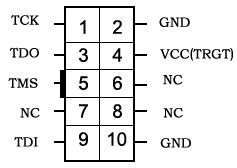
The basic JTAG interface consists of four signals:
- TDI (Test Data In): Serial data input to the TAP.
- TDO (Test Data Out): Serial data output from the TAP.
- TMS (Test Mode Select): Controls the state transitions of the TAP controller.
- TCK (Test Clock): Clock signal that synchronizes the JTAG operations.
To perform a JTAG operation, the following steps are typically followed:
- The TAP controller is reset by setting TMS high for five or more TCK cycles.
- An instruction is shifted into the Instruction Register (IR) through TDI by manipulating TMS and applying the appropriate number of TCK cycles.
- The instruction is decoded, and the corresponding data register is selected.
- Data is shifted into or out of the selected data register through TDI and TDO, respectively, by applying the appropriate number of TCK cycles.
- The process is repeated as needed to complete the desired testing, debugging, or programming operation.

Benefits of JTAG
JTAG offers several key benefits for testing, debugging, and programming electronic circuits and chips:
- Standardization: JTAG is a widely adopted industry standard, ensuring compatibility across different devices and tools.
- Non-intrusive testing: JTAG allows testing and debugging of a chip or board without requiring physical access to the internal components.
- Boundary-scan testing: JTAG enables testing of the interconnections between chips on a board, helping to identify manufacturing defects and short circuits.
- In-system programming (ISP): JTAG can be used to program devices such as flash memories and CPLDs while they are already mounted on a board.
- Debug and trace capabilities: JTAG can be used to access internal debug and trace features of a chip, facilitating software debugging and performance analysis.

JTAG Applications
JTAG has a wide range of applications in the electronics industry, including:
- Manufacturing test: JTAG is used to test PCBs and ICs for manufacturing defects, ensuring the quality and reliability of the final product.
- Board-level debugging: JTAG allows engineers to debug hardware issues on a board by accessing and controlling individual pins and internal registers of the chips.
- In-system programming: JTAG enables programming of devices such as flash memories, CPLDs, and FPGAs while they are already soldered onto a board, reducing the need for separate programming fixtures.
- Boundary-scan testing: JTAG is used to test the interconnections between chips on a board, helping to identify short circuits, open circuits, and other manufacturing defects.
- Software debugging: JTAG can be used to access the debug features of microprocessors and microcontrollers, enabling developers to debug embedded software and analyze performance issues.

JTAG Tools and Equipment
To work with JTAG, engineers and technicians use a variety of tools and equipment, including:
- JTAG programmers: Devices that connect to the JTAG TAP and provide an interface for programming, debugging, and testing chips and boards.
- JTAG debuggers: Tools that use JTAG to access the debug features of microprocessors and microcontrollers, enabling software debugging and performance analysis.
- Boundary-scan test systems: Automated test equipment (ATE) that uses JTAG to perform boundary-scan testing of PCBs and ICs.
- JTAG-enabled development boards: Evaluation and development boards that include JTAG interfaces for programming and debugging the onboard chips.
- JTAG software: Computer programs that provide a user interface for controlling JTAG operations, such as programming, debugging, and testing.
JTAG Standards and Variants
While IEEE 1149.1 is the most widely used JTAG standard, there are several other standards and variants that build upon or extend its functionality:
- IEEE 1149.6: Extends JTAG to support advanced I/O testing for high-speed differential signals.
- IEEE 1149.7: Defines a compact JTAG interface with reduced pin count and power consumption for use in small, low-power devices.
- IEEE 1149.8.1: Specifies a JTAG interface for testing high-speed source-synchronous buses.
- IEEE 1532: Defines a standard for in-system programming of programmable devices using JTAG.
- ARM Serial Wire Debug (SWD): A two-wire debug interface used by ARM Cortex processors, which is based on JTAG but uses fewer signals.
Implementing JTAG in a Design
To implement JTAG in a digital design, engineers must consider several factors:
- JTAG chain architecture: The arrangement of the JTAG-enabled devices in a daisy-chain configuration, with the TDO of one device connected to the TDI of the next.
- JTAG TAP controller: The design of the TAP controller state machine, which interprets the commands and data received through the TAP and executes the appropriate actions.
- Instruction register: The definition of the JTAG instructions supported by each device, and the corresponding opcodes.
- Data registers: The design of the data registers associated with each JTAG instruction, such as the Boundary Scan Register (BSR) and BYPASS register.
- Boundary-scan cells: The placement of boundary-scan cells between each pin and the internal logic of the chip, enabling control and observation of the pin states.
- JTAG I/O: The physical implementation of the JTAG interface signals (TDI, TDO, TMS, TCK) and their connection to the TAP.
Here’s an example of a simple JTAG chain architecture with three devices:
TDI --> [Device 1] --> [Device 2] --> [Device 3] --> TDO
         |              |              |
         TMS            TMS            TMS
         |              |              |
         TCK            TCK            TCK
In this configuration, the TDO of each device is connected to the TDI of the next device in the chain, forming a serial data path. The TMS and TCK signals are connected in parallel to all devices, ensuring that the TAP controllers are synchronized and receive the same commands simultaneously.
JTAG Security Considerations
While JTAG provides valuable benefits for testing, debugging, and programming, it can also introduce security risks if not properly managed. Unauthorized access to the JTAG interface could allow an attacker to read or modify sensitive data, bypass security features, or even take control of the device.
To mitigate these risks, designers can implement various security measures, such as:
- JTAG access control: Implementing authentication mechanisms or physical access controls to prevent unauthorized access to the JTAG interface.
- JTAG encryption: Encrypting the data transferred through the JTAG interface to protect against eavesdropping and tampering.
- JTAG lockout: Providing a means to disable the JTAG interface permanently or temporarily, such as through the use of security fuses or software-controlled disable mechanisms.
- Secure JTAG protocols: Using secure JTAG protocols, such as IEEE 1149.1-2013 (JTAG 2.0), which includes features like authentication, encryption, and access control.
- Secure coding practices: Following secure coding guidelines and performing security audits to identify and mitigate vulnerabilities in the JTAG implementation and associated software.
JTAG Boundary Scan Example
To illustrate the use of JTAG for boundary-scan testing, consider a simple example of a board with two chips connected by a trace:
[Chip 1] ------- Trace ------- [Chip 2]
To test the integrity of the connection between the two chips, we can use JTAG to perform a boundary-scan test:
- The boundary-scan cells of both chips are placed in their test mode, allowing them to be controlled and observed through the JTAG interface.
- A known test pattern is shifted into the boundary-scan cells of Chip 1 through the JTAG TDI.
- The test pattern is applied to the output pin of Chip 1, which is connected to the trace.
- The input pin of Chip 2, which is connected to the other end of the trace, captures the value on the trace.
- The captured value is shifted out of the boundary-scan cells of Chip 2 through the JTAG TDO and compared to the expected value.
- If the captured value matches the expected value, the trace is deemed to be functioning correctly. If not, a fault is detected, indicating a potential manufacturing defect or damage to the trace.
This example demonstrates how JTAG can be used to test the interconnections between chips on a board without requiring physical access to the trace or pins.
JTAG vs. other debug and programming interfaces
JTAG is not the only debug and programming interface available for electronic devices. Some other common interfaces include:
- Serial Wire Debug (SWD): A two-wire debug interface used by ARM Cortex processors, which is based on JTAG but uses fewer signals.
- Background Debug Mode (BDM): A debug interface used by some Freescale (now NXP) microcontrollers.
- In-Circuit Serial Programming (ICSP): A programming interface used by some Microchip PIC microcontrollers.
- Serial Peripheral Interface (SPI): A general-purpose synchronous serial interface that can be used for programming and debugging in some cases.
- Universal Serial Bus (USB): A widely used interface that can be used for debugging and programming through protocols like USB DFU (Device Firmware Update) or proprietary vendor-specific protocols.
While these interfaces serve similar purposes to JTAG, they each have their own unique characteristics, advantages, and limitations. JTAG remains one of the most widely used and standardized interfaces for debug and programming due to its versatility, robustness, and broad industry support.
Conclusion
JTAG is a powerful and versatile interface that has become an essential tool for engineers and technicians working with digital electronics. Its ability to provide non-intrusive access to the internal sub-systems of chips and boards has revolutionized the way we test, debug, and program electronic devices.
As electronic systems continue to grow in complexity and sophistication, the importance of JTAG will only continue to increase. By understanding the principles, applications, and best practices associated with JTAG, engineers can design more reliable, secure, and maintainable electronic products.
Frequently Asked Questions (FAQ)
1. What does JTAG stand for?
JTAG stands for Joint Test Action Group, which is the name of the industry group that developed the IEEE 1149.1 standard for boundary-scan testing.
2. What are the main benefits of using JTAG?
The main benefits of using JTAG include:
– Non-intrusive testing and debugging of chips and boards
– Boundary-scan testing to detect manufacturing defects and interconnect issues
– In-system programming of devices like flash memories and CPLDs
– Access to internal debug and trace features of chips for software debugging
3. How many signals are used in a typical JTAG interface?
A typical JTAG interface consists of four signals: TDI (Test Data In), TDO (Test Data Out), TMS (Test Mode Select), and TCK (Test Clock). Some variants, like IEEE 1149.7, may use fewer signals.
4. Can JTAG be used for programming devices?
Yes, JTAG can be used for in-system programming (ISP) of devices like flash memories, CPLDs, and FPGAs. This allows these devices to be programmed while they are already soldered onto a board.
5. What are some security risks associated with JTAG, and how can they be mitigated?
Unauthorized access to the JTAG interface could allow an attacker to read or modify sensitive data, bypass security features, or take control of the device. To mitigate these risks, designers can implement security measures like JTAG access control, encryption, lockout mechanisms, secure protocols, and secure coding practices.

No responses yet