Understanding PCB Schematic Netlists
A PCB (printed circuit board) schematic netlist is a crucial document that lists all the components and their interconnections on a PCB. It serves as a bridge between the schematic design and the physical layout of the PCB. The netlist contains information about each component, including its reference designator, value, and the nets (electrical connections) it is connected to.
Why are PCB Schematic Netlists Important?
PCB schematic netlists play a vital role in the PCB design process for several reasons:
-
Design verification: The netlist allows for verifying that the schematic design matches the intended circuit functionality. It helps catch errors or omissions in the schematic before proceeding to the PCB layout stage.
-
Bill of Materials (BOM) generation: The netlist contains a complete list of all components used in the design, which can be used to generate a Bill of Materials (BOM). The BOM is essential for procurement and manufacturing purposes.
-
PCB layout: The netlist provides the necessary information for the PCB layout software to create the physical board design. It defines how components are connected, enabling the software to route traces and place components accurately.
-
Design collaboration: Netlists facilitate collaboration between different teams involved in the PCB design process. They provide a standard format for exchanging design information, ensuring consistency and minimizing errors.
Elements of a PCB Schematic Netlist
A typical PCB schematic netlist consists of the following elements:
-
Header: The header section provides general information about the netlist, such as the file format version, date, and any comments or notes.
-
Component list: This section lists all the components used in the design. Each component entry includes the following information:
- Reference designator: A unique identifier for the component (e.g., R1, C2, U1).
- Component type: The type of component (e.g., resistor, capacitor, integrated circuit).
- Value or part number: The value of the component (e.g., 10K, 100nF) or its manufacturer part number.
-
Footprint: The physical package or footprint of the component.
-
Net list: The net list section defines the interconnections between components. Each net (electrical connection) is listed along with the component pins it connects. Nets are typically named based on their function or signal name (e.g., VCC, GND, DATA).
-
Footer: The footer section may contain additional information or closing statements.
Here’s an example of a simple PCB schematic netlist:
(export (version D)
  (design
    (source "example.sch")
    (date "2023-06-20")
    (tool "EDA Tool")
  )
  (components
    (comp (ref R1)
      (value 10K)
      (footprint Resistor_SMD:R_0805_2012Metric)
    )
    (comp (ref C1)
      (value 100nF)
      (footprint Capacitor_SMD:C_0805_2012Metric)
    )
    (comp (ref U1)
      (value LM358)
      (footprint Package_SO:SOIC-8_3.9x4.9mm_P1.27mm)
    )
  )
  (nets
    (net (code 1) (name "VCC")
      (node (ref U1) (pin 8))
      (node (ref R1) (pin 1))
    )
    (net (code 2) (name "GND")
      (node (ref U1) (pin 4))
      (node (ref C1) (pin 2))
    )
    (net (code 3) (name "IN")
      (node (ref U1) (pin 3))
      (node (ref R1) (pin 2))
    )
    (net (code 4) (name "OUT")
      (node (ref U1) (pin 1))
      (node (ref C1) (pin 1))
    )
  )
)
In this example, the netlist defines three components (R1, C1, and U1) and four nets (VCC, GND, IN, and OUT). The component list provides information about each component, including its reference designator, value, and footprint. The net list specifies the connections between the component pins.
Netlist Formats
PCB schematic netlists can be generated in various formats, depending on the EDA (Electronic Design Automation) software used. Some common netlist formats include:
- PADS: Used by the Pads PCB design software.
- OrCAD: Compatible with OrCAD and Allegro PCB design tools.
- PCAD: Used by PCAD PCB design software.
- Protel: Supported by Altium Designer and CircuitMaker.
- KiCad: Native format for the open-source KiCad EDA software.
Each netlist format has its own syntax and structure, but they all serve the same purpose of representing the components and interconnections of a PCB design.

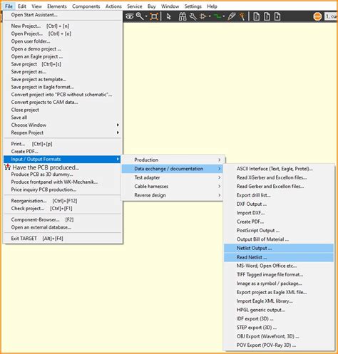
Generating PCB Schematic Netlists
Most EDA software tools provide functionality to generate PCB schematic netlists automatically from the schematic design. The process typically involves the following steps:
- Create the schematic design using the EDA software’s schematic editor.
- Assign appropriate component values, footprints, and reference designators.
- Define the net names and connections between components.
- Use the software’s netlist generation feature to export the netlist in the desired format.
It’s important to review the generated netlist to ensure accuracy and completeness before proceeding to the PCB layout stage.
Netlist Verification and Debugging
After generating the PCB schematic netlist, it’s crucial to verify its integrity and identify any potential issues. Some common verification steps include:
- Component and net count: Check if the number of components and nets in the netlist matches the schematic design.
- Connectivity check: Verify that all expected connections between components are present in the netlist.
- Component properties: Ensure that component values, footprints, and reference designators are correct.
- Electrical rule check (ERC): Perform an ERC to identify any electrical violations or potential design issues.
If any discrepancies or errors are found during the verification process, they should be investigated and resolved before moving forward with the PCB layout.
Best Practices for PCB Schematic Netlists
To ensure a smooth and efficient PCB design process, consider the following best practices when working with PCB schematic netlists:
-
Consistent naming conventions: Use clear and consistent naming conventions for components, nets, and other elements in the schematic and netlist. This helps improve readability and reduces the risk of errors.
-
Proper component selection: Choose appropriate component values and footprints based on the design requirements and manufacturing constraints. Ensure that the selected components are available and suitable for the intended application.
-
Schematic organization: Organize the schematic in a logical and hierarchical manner, using functional blocks and clear signal flow. This makes the schematic easier to understand and troubleshoot.
-
Documentation: Provide clear and concise documentation along with the netlist, including any design notes, assumptions, or special requirements. This helps other team members or manufacturers understand the design intent.
-
Version control: Implement version control for schematic and netlist files to track changes and collaborate effectively with other team members.
-
Design review: Conduct thorough design reviews at various stages of the PCB design process, including the schematic and netlist stages. This helps catch any issues early and ensures the design meets the specified requirements.
By following these best practices, you can create accurate and reliable PCB schematic netlists that facilitate a smooth transition to the PCB layout phase.
FAQ
-
What is a PCB schematic netlist?
A PCB schematic netlist is a text file that lists all the components and their interconnections in a PCB design. It serves as an intermediate representation between the schematic design and the physical PCB layout. -
Why is a PCB schematic netlist important?
A PCB schematic netlist is important because it: - Allows for verifying the schematic design against the intended circuit functionality.
- Helps generate a Bill of Materials (BOM) for procurement and manufacturing.
- Provides the necessary information for the PCB layout software to create the physical board design.
-
Facilitates collaboration and information exchange between different teams involved in the PCB design process.
-
What information does a PCB schematic netlist contain?
A PCB schematic netlist typically contains the following information: - Header section with general information about the netlist.
- Component list with details such as reference designators, component types, values, and footprints.
- Net list defining the interconnections between components and their respective pins.
-
Footer section with additional notes or closing statements.
-
What are some common netlist formats?
Some common PCB schematic netlist formats include: - PADS
- OrCAD
- PCAD
- Protel
-
KiCad
Each format has its own syntax and structure but serves the same purpose of representing the components and interconnections of a PCB design. -
How can I verify the accuracy of a PCB schematic netlist?
To verify the accuracy of a PCB schematic netlist, you can: - Check the component and net count against the schematic design.
- Verify the connectivity between components.
- Ensure component values, footprints, and reference designators are correct.
- Perform an Electrical Rule Check (ERC) to identify any electrical violations or potential design issues.
If any discrepancies or errors are found, they should be investigated and resolved before proceeding with the PCB layout.
| Element | Description |
|---|---|
| Header | General information about the netlist (version, date, tool) |
| Component List | List of components with reference designators, values, footprints |
| Net List | Defines interconnections between components and their pins |
| Footer | Additional notes or closing statements |
Sample PCB Schematic Netlist Elements
By understanding the purpose, structure, and best practices associated with PCB schematic netlists, designers can create accurate and reliable designs that seamlessly transition from schematic to PCB layout. Effective management of netlists streamlines the design process, reduces errors, and ensures the final PCB meets the intended functionality and performance requirements.
No responses yet