What is Electrostatic Discharge (ESD)?
ESD occurs when there is a significant difference in electrical potential between two objects and this potential difference is rapidly equalized through a sudden flow of current. Some common examples of ESD include:
- The shock you feel when touching a doorknob after walking across a carpeted floor
- The crackling sound when taking off a sweater
- A lightning strike
The buildup of electrical charge that leads to ESD can be caused by triboelectric charging (friction between materials), induction (charge redistribution due to an external electric field), or conduction (charge transfer through direct contact).
ESD Voltage Levels
The voltage levels involved in ESD events can be extremely high, often reaching several kilovolts (kV). The table below shows some typical ESD voltage levels generated by various activities:
| Activity | Typical Voltage Range |
|---|---|
| Walking across a carpet | 1,000 to 35,000 V |
| Walking across a vinyl floor | 250 to 12,000 V |
| Worker at a bench | 700 to 6,000 V |
| Picking up a plastic bag from a bench | 1,200 to 20,000 V |
| Sitting in a chair with urethane foam pad | 1,500 to 18,000 V |
Source: ANSI/ESD S20.20-2014
How ESD Affects Electronic Components and PCBs
Electronic components, especially semiconductor devices, are highly susceptible to ESD damage due to their small size and low operating voltages. When an ESD event occurs, the high voltage and current can cause various types of damage, including:
- Oxide breakdown: The thin gate oxide in MOS devices can rupture due to the high electric field, causing permanent damage.
- Junction damage: The p-n junctions in semiconductor devices can be damaged by the high current, leading to increased leakage or shorts.
- Metallization melt: The metal interconnects in ICs can melt or vaporize due to the high current density, causing open circuits.
- Charge injection: ESD can inject charge into the device, causing temporary or permanent changes in its behavior.
PCBs can also suffer from ESD damage, primarily through the failure of the components mounted on them. Additionally, ESD can cause damage to the PCB itself, such as:
- Delamination of the board materials
- Carbonization of the insulating layers
- Overcurrent damage to traces and vias
ESD Protection Strategies for PCB Design
To minimize the risk of ESD damage in PCB designs, several protection strategies can be employed:
1. Component Selection
Choose components with built-in ESD protection whenever possible. Many modern ICs come with on-chip ESD protection structures such as diodes, transistors, or silicon-controlled rectifiers (SCRs). These devices are designed to clamp the voltage during an ESD event and shunt the current away from the sensitive circuitry.
2. PCB Layout
Proper PCB layout techniques can help reduce the impact of ESD:
- Placement: Place ESD-sensitive components away from the board edges and connectors, where ESD events are more likely to occur.
- Grounding: Provide a low-impedance path to ground for ESD currents by using wide, short traces and multiple vias.
- Guard rings: Use grounded guard rings around sensitive components to provide a preferred path for ESD currents.
- Shielding: Use shielding techniques, such as grounded metal enclosures or conductive coatings, to protect sensitive areas of the PCB.
3. ESD Protection Devices
Incorporate dedicated ESD protection devices into the PCB design. These devices are specifically designed to absorb and dissipate the energy from an ESD event, protecting the sensitive components. Some common types of ESD protection devices include:
- Transient voltage suppressors (TVS): These devices clamp the voltage to a safe level during an ESD event and are available in various configurations, such as diodes, arrays, and polymers.
- Gas discharge tubes (GDTs): GDTs are high-capacity devices that can handle large ESD currents. They consist of a gas-filled chamber that ionizes during an ESD event, providing a low-impedance path to ground.
- Metal oxide varistors (MOVs): MOVs are voltage-dependent resistors that offer high resistance at normal operating voltages but switch to a low-resistance state during an ESD event, shunting the current to ground.
The table below compares some key characteristics of these ESD protection devices:
| Device Type | Typical Capacitance | Typical Clamping Voltage | Response Time |
|---|---|---|---|
| TVS Diode | 0.5 to 10 nF | 5 to 400 V | < 1 ns |
| GDT | 0.5 to 2 pF | 75 to 1000 V | 100 ns to 1 μs |
| MOV | 10 to 10,000 pF | 11 to 1800 V | 1 to 50 ns |
Source: Various manufacturer datasheets
4. Handling and Assembly Procedures
Implementing proper ESD handling and assembly procedures is essential to protect PCBs and components from damage during manufacturing and use. Some key practices include:
- Using grounded wrist straps, work surfaces, and floor mats
- Wearing ESD-safe clothing and footwear
- Using ionizers to neutralize charges on insulating materials
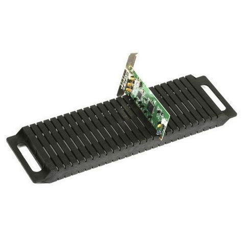
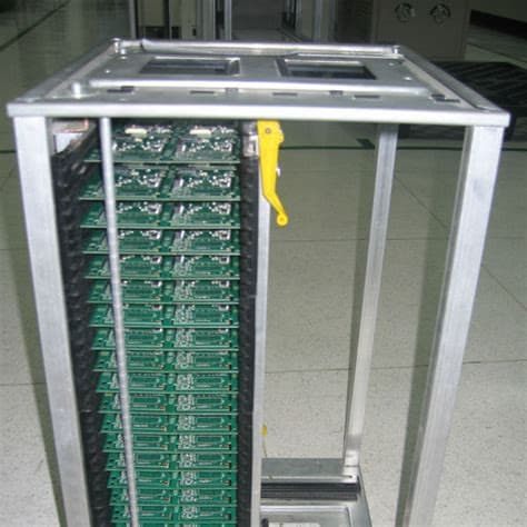
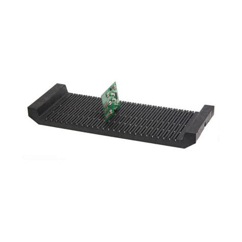
- Storing and transporting PCBs and components in ESD-safe packaging

Testing and Verification
After implementing ESD protection measures in a PCB design, it is crucial to test and verify their effectiveness. Several standards, such as the IEC 61000-4-2 and the ANSI/ESD S20.20, provide guidelines for ESD testing and qualification.
ESD testing typically involves applying high-voltage pulses to the device under test (DUT) and monitoring its response. The test levels and waveforms are specified in the relevant standards. Some common ESD test methods include:
- Human Body Model (HBM): Simulates the discharge from a human body to a device, with typical test voltages ranging from 2 to 8 kV.
- Machine Model (MM): Simulates the discharge from a machine to a device, with typical test voltages ranging from 100 to 400 V.
- Charged Device Model (CDM): Simulates the discharge from a charged device to ground, with typical test voltages ranging from 250 to 2000 V.
By performing ESD testing and qualification, designers can ensure that their PCBs and products meet the necessary reliability and robustness requirements.
Frequently Asked Questions (FAQ)
-
Q: What is the difference between ESD and EMI?
A: ESD (Electrostatic Discharge) refers to a single, fast, high-current transfer of electrostatic charge, while EMI (Electromagnetic Interference) refers to ongoing electromagnetic disturbances that can interfere with the normal operation of electronic devices. -
Q: Can ESD damage occur without visible signs?
A: Yes, ESD damage can occur without visible signs, especially in the case of latent or hidden failures. These failures may not be immediately apparent but can manifest over time, leading to reduced reliability or premature device failure. -
Q: What is the most common cause of ESD damage during PCB assembly?
A: The most common cause of ESD damage during PCB assembly is improper handling of sensitive components by assembly personnel. This can be mitigated by implementing proper ESD-safe handling procedures, such as using grounded wrist straps and work surfaces. -
Q: Can software be used to simulate and analyze ESD in PCB designs?
A: Yes, several software tools, such as ANSYS SIwave, Cadence Allegro PCB SI, and Mentor Graphics HyperLynx, offer ESD simulation and analysis capabilities. These tools can help designers identify potential ESD vulnerabilities and optimize protection strategies. -
Q: Are there any industry standards that govern ESD protection in PCB design?
A: Yes, several industry standards provide guidelines and requirements for ESD protection in PCB design and manufacturing. Some key standards include ANSI/ESD S20.20, IEC 61000-4-2, and JEDEC JS-001. These standards cover various aspects of ESD protection, such as component selection, PCB layout, handling procedures, and testing methods.
Conclusion
Electrostatic discharge (ESD) is a significant concern in PCB design, as it can cause damage to sensitive electronic components and lead to reduced reliability or complete device failure. By understanding the nature of ESD and implementing appropriate protection strategies, such as selecting components with built-in protection, optimizing PCB layout, incorporating dedicated ESD protection devices, and following proper handling and assembly procedures, designers can significantly reduce the risk of ESD damage in their products.
Additionally, thorough testing and verification using industry-standard methods can help ensure that PCBs and products meet the necessary ESD reliability and robustness requirements. As electronic devices continue to become smaller, faster, and more complex, the importance of effective ESD protection in PCB design will only continue to grow.
No responses yet